
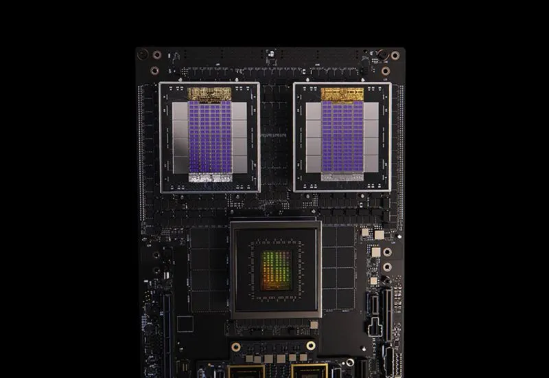
Nvidia plans to bring Feynman-based computing accelerators to market in the second half of 2028, and sources in Taiwan say preparations for the debut are accelerating, putting higher demands on the company’s contractors to prepare for the new technology. In addition to TSMC’s A16 process technology, this also means new chip packaging methods.
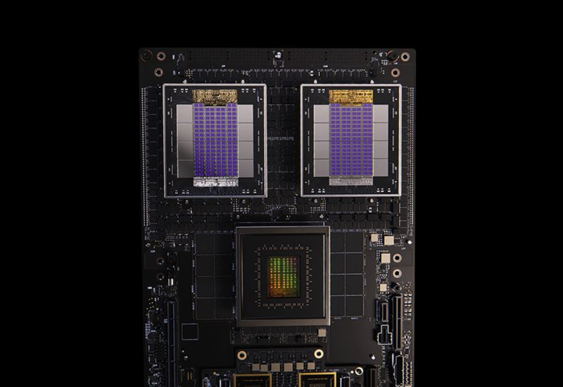
Image source: NVIDIA
The latter includes co-packaging of 3D SoIC layout and optical interconnect (CPO), e.g. digital age. For Taiwan Semiconductor Manufacturing Co., Ltd., this means it must speed up the construction of AP7 and AP8 factories, which will use the SoIC method to process wafers. They originally expected to be able to process 20,000 wafers per month by the end of 2026, but now the plan has been revised to speed up the process and that number will increase to 50,000 wafers per month by the end of 2027. The installation of public facilities, the construction of “clean rooms” and the installation of equipment in these TSMC factories are all forced to be carried out in advance.
In addition to using A16 process technology, the Feynman accelerator also means 3D SoIC integration technology, the use of customized HBM-type memory and co-package (CPO) optical connections. Nvidia’s needs have already determined the pace of technology development for TSMC and its closest partners. At the same time, SoIC 3D packaging technology will also be in demand from TSMC’s other customers, so accelerating expansion in this field will benefit the company to a certain extent.
In the case of TSMC’s 2nm technology, things were going well and Apple’s A20 Pro processors were manufactured using it in sufficient quantities and defect levels, but with the integration of DRAM memory, problems arose due to shortages. As a result, TSMC now has a backlog of around $1 billion worth of A20 Pro processors waiting to install memory chips. This packaging technology was specifically adapted to Apple’s needs and compared to the mobile version of CoWoS.
For Microsoft, TSMC plans to produce more than 300,000 Maia 300 chips by the end of next year, showing the cloud giant’s growing demand for AI-specific chips. Starting from the second half of this year, TSMC will also begin to use the CPO method to expand chip packaging production capacity so that it can support optical connection integration with information transmission rates up to 400 TB/s.
If you find an error, select it with your mouse and press CTRL+ENTER.