
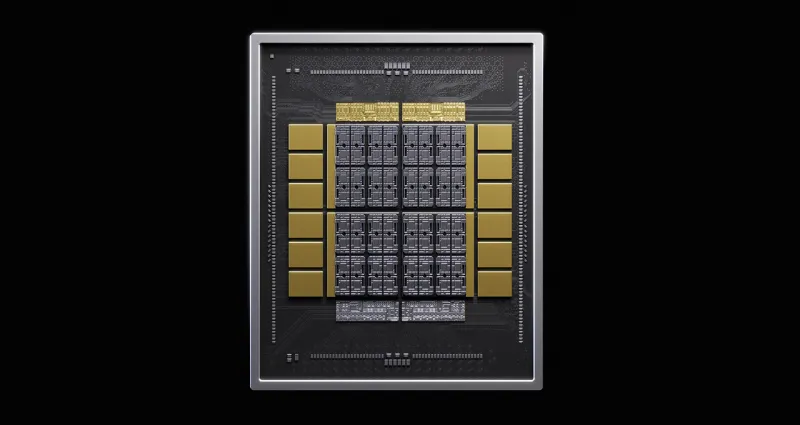
With the development of the AI agent market and the active deployment of AI models with trillions of parameters, the performance of supporting AI infrastructure requires not only improved computing power, but also efficient design within a single system of computing, memory, network, and software. Assisting hyperscalers and other customers NVLink Fusionthe company offers NVHBM memory.
In traditional architecture, the HBM controller is located on the XPU chip and occupies some area available for computing. NVHBM uses the same technology that NVIDIA will use in its future GPUs – a custom memory controller integrated into the main HBM die, so NVHBM will provide up to 30% more memory bandwidth and up to 15% less power consumption compared to standard memory, and will also free up up to 25% of the main XPU die. HBM4E.
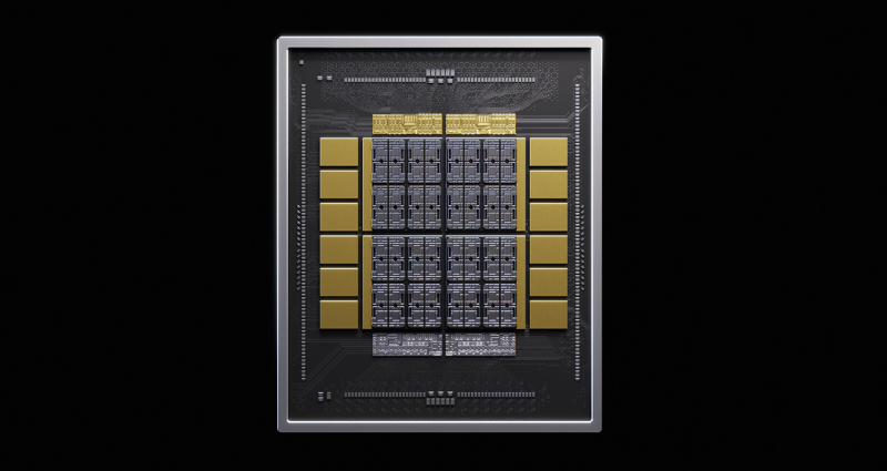
Image source: NVIDIA
Several memory vendors will provide standard NVHBM implementations. This should reduce the engineering effort required to integrate and certify memories from different manufacturers. NVLink Fusion customers will be able to bring customized AI accelerators to market faster. As part of a broader NVLink Fusion collaboration with NVIDIA, Amazon’s Annapurna Labs will be the first lab dedicated to NVHBM to integrate NVLink Fusion into AI accelerators. Training 4.
NVLink Fusion already allows you to connect XPUs and CPUs to NVIDIA rack platforms, and the company’s partners have access to NVLink-C2C small form factors, NVLink network switches and racks NVIDIA MGX. A variety of CPUs from different partners, ASIC developers, etc. are also available.
source: