
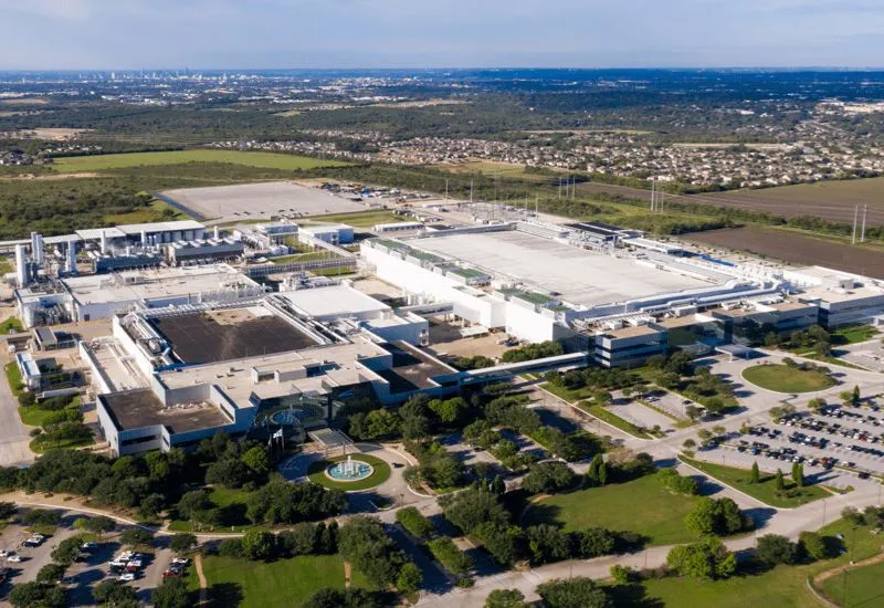
The construction progress of Samsung Electronics’ new chip foundry plant in Texas has been significantly accelerated after Samsung Electronics reached an agreement with Tesla of the United States to produce 2-nanometer wafers at the plant to meet the latter’s needs. By the time it is put into production, it will be fully loaded with orders from Broadcom and Arm, and Samsung has also opened a research center in Japan.
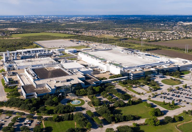
Image source: Samsung Electronics
According to Korean media reports, TrendForce. Samsung’s first factory in Tyler, Texas, will start producing trial products in late September or early October and will not reach mass production until 2027. It is expected to initially process 50,000 silicon wafers per month. In addition to producing AI5 and AI6 chips for Tesla, it can also produce chips for orders from Broadcom and Arm. The latter has historically only been involved in the development of processor architectures, but has recently made the strategic decision to provide processors under its own brand. Apparently, by that time, TSMC’s production capacity has been retained for many years, and the British holding company does not want to share its developments with Intel, so Samsung is likely to become a contract manufacturer of the brand’s chips.
Samsung is also making progress on its second factory in Tyler. Construction will begin before the end of this year, with the product being able to be mass-produced by the end of this decade. On-site “zero circulation” construction work has begun, and negotiations with the second enterprise equipment supplier are also in full swing. Samsung’s Texas project is progressing faster than originally planned.
Along the way, this week in Yokohama, Japan is open Samsung Research Center will focus on developing chip packaging technology that can be used in artificial intelligence infrastructure. There are many companies specializing in wafer packaging materials and equipment in the local market, so the choice of location for the Samsung Research Center is logical. A test laboratory will be set up here to allow testing of wafer packaging technology under production-like conditions. Samsung invested a total of US$257 million in the construction of the center, more than half of which came from subsidies from the Japanese government. 95 researchers from Japan and South Korea will work here.
Representatives of 15 large Japanese companies attended the center’s unveiling ceremony. Even in the production of HBM memory, Samsung relies heavily on Japanese suppliers, so localized professional interaction should be beneficial to Korean manufacturers in any case and accelerate the development of new products. Samsung cooperates with more than 50 Japanese companies to produce advanced artificial intelligence infrastructure chips.
If you find an error, select it with your mouse and press CTRL+ENTER.