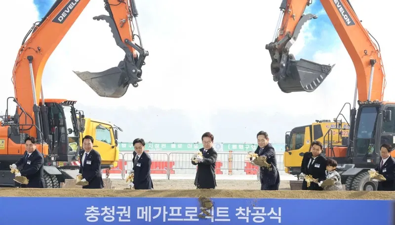
This summer, South Korean authorities called investment in AI and chips urgent. Today, Samsung began to implement these plans by laying the foundation stone for a new giant complex for the production of memory for AI.
Image Source: Samsung
Construction was started with the participation of South Korean President Lee Jae Myung and Chairman of the Board of Directors of Samsung Electronics Lee Jae-yong. Work formally began on November 12, 2026 on the Samsung campus in Onyang, Asan city, Chungcheong province.
The project will be part of a large-scale program for the development of the semiconductor industry and artificial intelligence infrastructure outside the capital region. Samsung intends to invest a total of ₩144 trillion (about $108 billion) in the development of its enterprises in Chuncheon province, including the production of semiconductors, displays, batteries and components for AI servers.
Directly at the Onyang site, the company plans to establish five production lines for the production and advanced packaging of HBM (High Bandwidth Memory) memory. Samsung Electronics’ total investment in this facility will amount to ₩46 trillion (approximately $34.5 billion): ₩6 trillion is provided for the construction of production facilities and another ₩40 trillion for the installation of modern technological equipment. The construction that has begun relates to the fifth production line. It will be a three-story building with clean rooms with a total area of approximately 31,000 m2. The launch of the facility is scheduled for June 2028, and its creation should provide about 700 permanent jobs.
Once the project is completed, the campus area will increase from the current 270,000 to 420,000 m2. The facility aims to transform Onyang from a site primarily focused on the assembly and testing of conventional semiconductors into one of HBM’s key centers for advanced packaging. This technology involves combining multiple layers of memory chips into a single high-density design, which allows for increased data throughput between memory and processor. Such solutions are especially in demand in artificial intelligence accelerators working with large amounts of data.
The construction in Onyan is just one element of a larger program. In July 2026, Samsung announced plans to invest ₩140 trillion in the development of high-tech production in Chuncheon, and by November the group’s total announced investments were increased to ₩144 trillion.
In parallel, the region plans to develop the production of advanced displays, batteries and components for AI servers, and projects from other companies, including SK hynix, will also be implemented. The South Korean government intends to support the initiative by investing in infrastructure and speeding up administrative permitting procedures. The start of construction of Samsung’s new factory complex in Onyang was actually the first in South Korea. megaproject worth ₩4.7 quadrillion ($3.5 trillion), aimed primarily at developing the artificial intelligence industry in the country.
If you notice an error, select it with the mouse and press CTRL+ENTER.