


Intel recently admitted that the 14A process will be the first stage of EUV lithography using high numerical aperture (High-NA) equipment, and the company began receiving components for the first sample of such equipment last year from ASML. Now it has become known that ASML specialists managed to launch the corresponding equipment in the Netherlands.
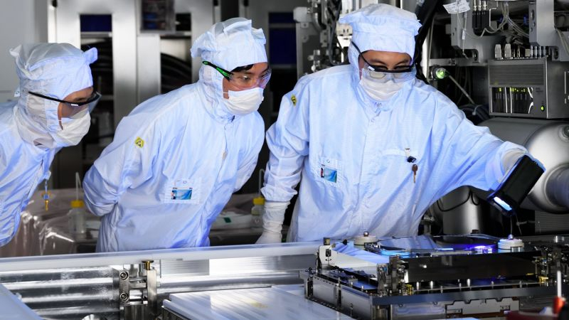
Image source: ASML
Ann Kelleher, who is responsible for technology development at Intel, confirmed during a conference in San Jose this week that the high numerical aperture equipment used for the experiments has begun work at the ASML laboratory, and the test silicon wafer has already been irradiated with his help. A copy of the ASML Twinscan EXE:5000 lithographic scanner with similar capabilities is currently being assembled at the Intel laboratory in Oregon, but judging by the Reuters publication, it is not yet ready for full-fledged operation.
Such equipment allows obtaining an optical resolution of up to 8 nm per exposure, which is noticeably better than conventional EUV scanners, which provide a resolution of 13.5 nm per exposure. While the equipment in the Netherlands is undergoing further calibration, it is not yet ready to process silicon wafers in order to obtain full-fledged test chips. It is assumed that after installing a similar scanner in Oregon, Intel will be able to begin similar experiments, moreover, within the framework of the Intel 18A technical process, although the corresponding equipment will begin to be used in mass production no earlier than 2026 within the framework of Intel 14A technology. By the end of 2027, the company expects to switch to the Intel 10A process technology, which will also use High-NA EUV equipment.
If you notice an error, select it with the mouse and press CTRL+ENTER.


