



Arm revealed details about its AGI server processor at the Hot Chips 2026 event, talking about its configuration and promising to start commercial shipments in the coming months.
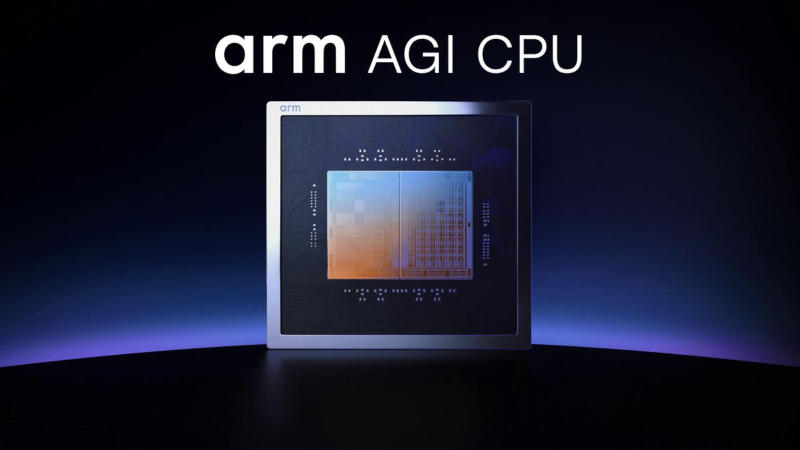
Image source: arm
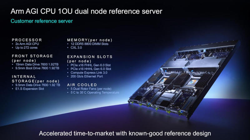
Arm AGI is a dual-chip data center processor available in 64, 128 or 136 Neoverse V3 core configurations with clock speeds ranging from 2.8 to 3.7 GHz. Physically, each dielet contains 70 cores, but some of these cores are reserved to increase the yield of suitable processors. The core has two 128-bit vector blocks and a 2MB L2 cache, and the total system cache capacity reaches 272MB.
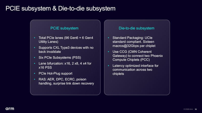
Each chiplet contains about 50 billion transistors and has its own six-channel DDR5 controller. The processor supports up to 6 TB of memory per socket and DDR5-8800, with a total bandwidth of up to 844.8 GB/s. The two chiplets are connected via UCIe with a transfer rate of 32 GT/s and a total throughput of approximately 2 TB/s.
To connect peripheral devices, Arm AGI provides 96 PCI Express 6.0 lanes (supports CXL 3.0, including memory expansion) and 4 PCI Express 4.0 lanes. In addition, I3C, I2C and SPI interfaces are also provided. The processor has an estimated thermal power of 300 W.
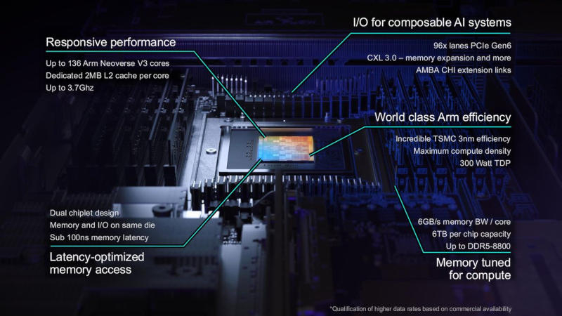
When designing AGI, Arm adopted a different approach to small-die packaging than AMD, Intel and Nvidia. Rather than allocating computing resources and I/O to a dedicated chiplet, each AGI chip has its own processor core, memory controller, and I/O components. As a result, local memory accesses do not have to be transferred to adjacent chiplets, reducing latency and improving performance for latency-sensitive tasks. Arm says DRAM access latency is less than 10 nanoseconds.
Each chiplet uses an 8 × 9 topology CMN-S3 interconnect network to connect processor cores, memory, I/O and accelerators. It also provides memory coherence between the two chiplets. If a core needs to access memory connected to an adjacent die, the request is transmitted over a consistent inter-die connection, although latency is expected to increase in this case.
CMN-S3 includes a decentralized system cache, Snoop filters, and HN-S (Home Node System) nodes that manage consistency and traffic. The processor has a total system cache of up to 272 MB. This architecture provides coherent communication not only within a single chiplet, but also between dies, allowing both halves of the AGI to operate as a single NUMA system.
Arm is paying special attention to the memory subsystem because AGI is positioned as a processor for AI servers and systems with AI agents, where high throughput and low latency are very important when processing large amounts of data. Two six-channel DDR5 controllers deliver up to 844.8 GB/s combined throughput, with available bandwidth shared between cores and I/O devices.
The AGI memory controller supports out-of-order instruction scheduling, optimal access allocation among DRAM groups, and programmable memory page management strategies. MPAM (Memory Partitioning and Monitoring) technology allows you to control and limit individual components’ access to memory bandwidth. There are also QoS-based traffic prioritization and congestion control mechanisms in the case of multiple cores and I/O devices competing for DRAM resources at the same time.
The memory subsystem also gains extensive RAS (Reliability, Availability, Serviceability) functionality, including correcting failures of individual DRAM dies, RowHammer protection, error recovery mechanisms, their registration and manual generation for testing.
Independent test results for Arm AGI have not yet been released. Arm claims that servers using the new processors will have twice the performance per rack compared to systems based on modern x86 processors. Commercial deliveries of Arm AGI are expected to begin in the coming months.
If you find an error, select it with your mouse and press CTRL+ENTER.