
Yuan✴ report New details about 667W AI accelerator 300 meters – The first chip optimized for training DLRM models. Unlike LLM, which requires huge floating point throughput, the recommended model faces the challenge of requiring fast and efficient accelerator communication as well as large memory capacity and high interconnect bandwidth.
Their embedding tables can contain more than 99% of model parameters, requiring hybrid parallelism resulting in frequent collective AllReduce, AllToAll, and AllGather operations on hundreds of accelerators. On chips such as GPUs, these communication operations compete with computing for the same resources, often resulting in inefficient use of expensive hardware.
In order to solve this problem, designers use the joint development of MTIA 300 and HCCL (a communication interface library based on the underlying hardware) to make communication the primary task of IC design. In fact, HCCL delivers up to 940 GB/s of data throughput in a single rack. On a model with 150 billion parameters running on 40 accelerators, the total communication time using MTIA 300 was 3.9 times faster than the equivalent GPU-based cluster.
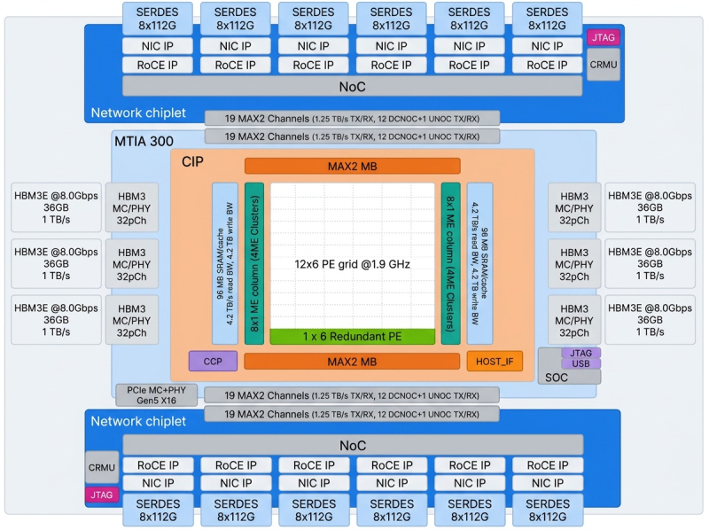
Image source: Meta✴
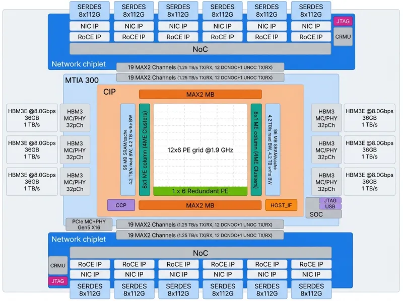
In MTIA 300, the network interface is located within the chip package itself. Two 5nm networking chipsets, each containing six dedicated 800GbE RoCE adapters, deliver 1.2 TB/s of total I/O throughput without crossing the PCIe bus. This eliminates the host-to-NIC bottleneck present in traditional GPU architectures, where the CPU must act as an intermediary between the accelerator and the network, and avoids PCIe congestion between the accelerator and NIC. At the same time, NIC can be flexibly used for expansion.
Because the same 12 Ethernet-based NICs are used for scale-up (within a 16-node rack, up to 1 TB/s) and scale-out (between racks, up to 200 GB/s), you have the flexibility to allocate NICs to meet changing needs. As model requirements change, the network rather than the hardware itself can be reconfigured. To minimize transaction delays, developers have introduced quick notifications (doorbells). Executing the request entry itself acts as an alert, eliminating additional memory reads and saving approximately 800 ns per operation.

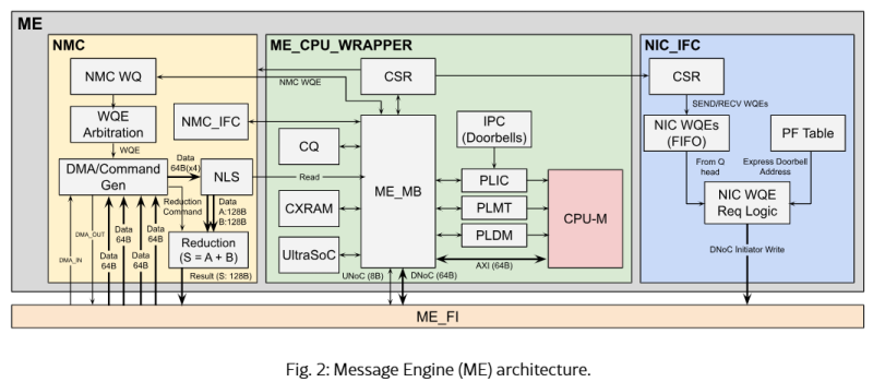
Image source: Meta✴
In the case of GPUs, libraries like NCCL implement collective communication operations in the form of cores that use the same resources required for training computations. The intersection of collective operations and learning operations causes both to slow down. MTIA 300 takes a different approach. In addition to a matrix of 72 3nm compute elements (PE), the chip also includes 16 dedicated message engines (ME) that handle all communications independently.
ME includes a RISC-V core for orchestration; a network interface that routes requests to the required NIC; and a near-memory computing (NMC) unit that performs reduction operations at 128 bytes/cycle. The NMC is located at the edge of the die, next to the HBM and cache, delivering a total of more than 2.8 TB/s of reduced throughput, more than twice the I/O throughput. This allows collective AllReduce and ReduceScatter operations to be performed at NIC line speed without using PE resources.

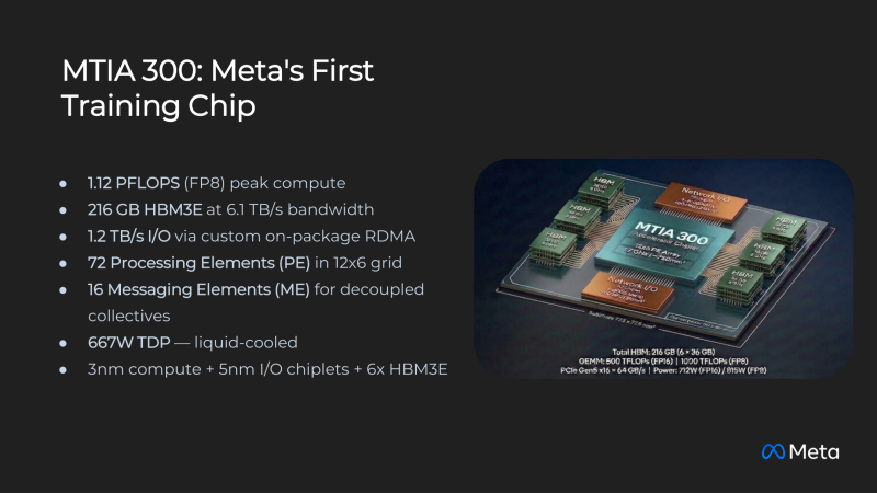
Image source: Meta✴
The result is nearly perfect operational isolation. Executing large-scale GEMM jobs and collective jobs simultaneously will result in a reduction of less than 0.5% in computing throughput, while traditional GPUs may reduce computing throughput by more than 20% because they use the same communication and computing resources.
Developed in conjunction with MTIA 300, HCCL, instead of managing communication with the host at runtime, compiles each collective operation into a complete set of subgraphs (arrays of task queues with explicit dependencies) that are sent to the ME for fully autonomous execution. In this way, the host only sends a set of network commands to the accelerator once and no longer interferes with the operation of the network.

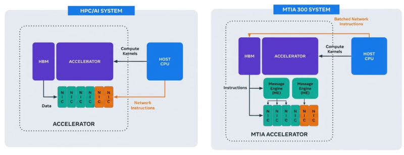
Image source: Meta✴
based on metadata✴an architecture that integrates naturally with PyTorch. Collective operations are compiled together with computational tasks into a single graph. The algorithm chosen by HCCL itself takes into account network topology and bandwidth asymmetry to minimize inter-rack traffic. Other reasoning methods were also developed: when PEs use explicit notifications, one-way communication, and to initiate collective operations in parallel based on signals from the core without interrupting the work of the latter.
The company points out that the MTIA 300 has other advantages: the 216 GB HBM3E (6.1 TB/s) allows you to put more data on a single die instead of loading it again from the outside; there is only one CPU per accelerator, which makes it possible to load intensive calculations at certain stages; and the high network bandwidth allows you to use higher-precision data formats when necessary.
Although the combination of modest FP performance and spacious and fast HBM in the MTIA 300 was originally optimized for DLRM training, these qualities enable the chip to be used effectively for a wider range of workloads, including inference of generative AI models. It is worth noting that the Meta method✴ Implementing NICs directly into the die itself is not new. For example, Intel/Habana chips Highest 2ndLaunching in 2022, using 24 100GbE RoCE interfaces for vertical and horizontal expansion.
source: