
Generally speaking, reducing the size of transistors and circuits has been an easy way to improve chip performance. All this works until the size of the element is very close to that of the atom. The physics of the material itself has arisen, and its electrical and physical properties no longer fulfill its mission – to accurately transmit electrical signals under complete control. Dielectrics are no exception and can fragment.
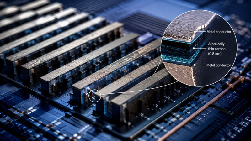
Image source: National University of Singapore
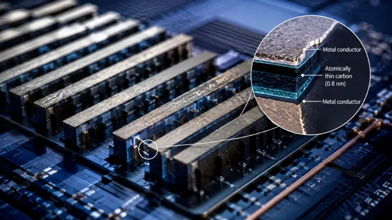
Dielectric and insulating material issues for atomic-level wafers, etc. study Scientist from Singapore. So researchers at the National University of Singapore (NUS) have created an ultra-thin carbon film with a thickness of just 0.8 nm that could help continue to reduce the size of computer chips. What’s most encouraging is that as early as this spring, they transferred this knowledge to engineers at Taiwan’s TSMC, who were tasked with solving the problem of putting their developments into industrial production.
Surprisingly, amorphous carbon exhibits an unusual combination of ultralow dielectric constant, high mechanical strength and the ability to block the diffusion of metal atoms—in fact, a set of fundamental properties that are becoming critical as wafers continue to be miniaturized. A combination that could simultaneously break through into future wafer production pipelines.
One of the problems with modern processors is not only the reduction in the number of transistors, but also the complication of the conductor system (metal connections between conductors). Inside an advanced chip, billions of transistors are connected through tiny copper wires, and the distance between them continues to shrink. If the packaging is too dense, parasitic capacitance will occur: adjacent lines start to interact with each other, increasing power consumption and slowing down signal transmission. To solve this problem, insulators with very low dielectric constants (low-k materials) are needed, but conventional porous dielectrics lose their mechanical stability at a thickness of a few nanometers and cannot be used in the future.
The material proposed by the scientists is a bond-based amorphous carbon sp type2. Even with a thickness of only 0.8 nm, it maintains a dielectric constant of about 1.35, which is close to the value of vacuum (1.0). At the same time, the film can withstand an electric field of 28-31 MV/cm, which significantly exceeds the performance of some promising ultrathin insulators such as amorphous boron nitride. Another advantage is its high hardness – about 100 GPa, which is about an order of magnitude higher than conventional silica.
In addition to insulating adjacent conductors, the carbon film also acts as a barrier against metal migration. Modern wafers often require a separate layer of tantalum nitride to prevent copper from leaching into surrounding materials, but this takes up valuable space. The new carbon material combines two functions: it reduces parasitic capacitance while preventing the movement of metal ions. Tests have shown that even a layer with a thickness of 0.8 nm has barrier properties that are 100 times superior to tantalum nitride, which is widely used in modern wafer production.
Using the chemical vapor deposition method, carbon films can be formed at a relatively low temperature of 300°C, and not only on flat substrates, but also on all irregularities and depressions, which also creates prospects for 3D layout of wafer components. As the world leader in semiconductor production, TSMC is likely to be the first to put this technology into practice, but so far these are just laboratory studies on small-diameter wafers, and how the technology will perform when scaled up remains an open question.
If you find an error, select it with your mouse and press CTRL+ENTER.