
TSMC discussed new wafer production technologies at SEMICON Taiwan 2026 to meet the growing demand for computing power in the AI ecosystem. The company focuses on new packaging and chip assembly technologies, and also develops silicon photonics technology directions.
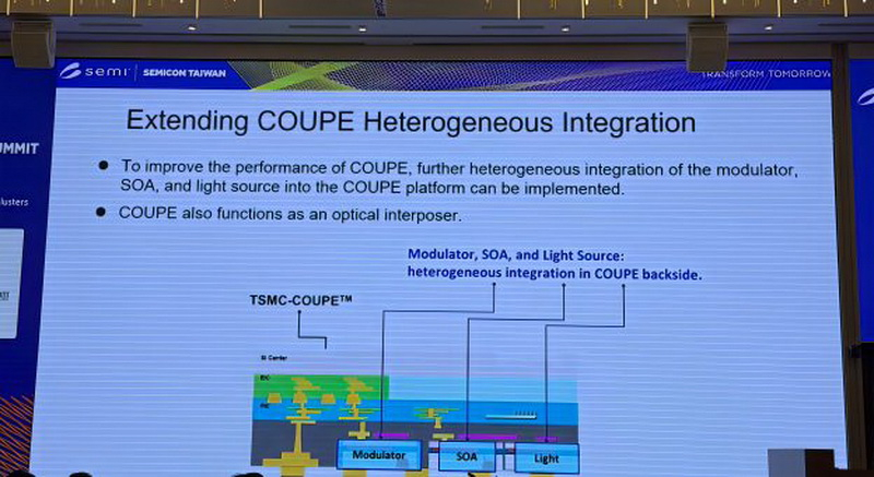
Image source: TSMC
Li April, head of global business development for artificial intelligence and high-performance computing at TSMC, said that the demand for artificial intelligence computing resources has increased fivefold every year, and the demand for computing power has also continued to increase. To this end, TSMC is integrating advanced process technology, 3D assembly technology and silicon photonics into its HPC solutions. The company expects that by 2029, the integration of advanced SoIC packaging and CoWoS packaging technologies will increase overall system performance by 50 times compared to technologies launched in 2024.
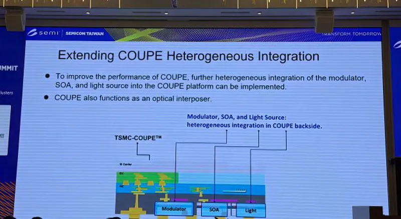
Lee believes that heterogeneous integration is the only way to overcome current computing limitations. TSMC plans to launch N2P-on-N3P 3D integration in 2026, followed by A14-on-A14 with 4.5μm interconnect pitch in 2029. The company also continues to develop its COUPE silicon photonics technology. Its 2-4 µm interconnect pitch reduces transmission loss to just 0.06 dB at 112 Gbps, while the micro-bump transmission loss is 1.38 dB, which helps reduce power consumption and latency to 10-20 nanoseconds.
TSMC’s COUPE (Compact Universal Photonic Engine) platform uses TSMC-SoIC interconnect technology to integrate electronic integrated circuits (EICs) and photonic integrated circuits (PICs), while supporting gate couplers (GC) and edge couplers (EC). In order to further increase production capacity, TSMC is pursuing two development directions. One of these is to increase the data transfer rate per channel from 200 Gbps to more than 400 Gbps, while increasing the number of channels from 16 to more than 128, which will increase the total throughput from 3.2 Tbps to more than 12.8 Tbps. The second direction involves extending wavelength division multiplexing (WDM) from a single wavelength to 4, 8, 16 or more.
As co-packaged optics (CPO) technology becomes more popular, the company is also solving test and design challenges. TSMC has launched wafer-level optical testing of edge-coupled components, allowing it to screen out defective wafers before expensive fiber assembly. The company also launched an optical semiconductor design platform that enables electron-photon coupling simulations to address key challenges in silicon photonics. The platform supports Cadence and Synopsys tools to help accelerate new product development.
KC Hsu, vice president of advanced packaging technology and services at TSMC, said that the optical transceiver architecture is undergoing structural changes and it is expected that silicon photonics will occupy more than 50% of the optical transceiver market in 2027. The next step will be to manufacture optical transceivers on silicon substrates, with some suppliers expected to start mass production in the second half of 2026.
Mr. Xu said that as the demand for high-speed communication links continues to grow, optics will become the “nervous system” of the data center. According to statistics, sales of optical modules will grow by 25% in 2025, and their supply is expected to grow by another 50% in 2026. At the same time, the market for high-performance transceivers with data transmission rates above 100 Gbit/s will double in 2024, and will grow by another 60% in 2025.
Hsu pointed out that Taiwan’s semiconductor manufacturing ecosystem has been able to produce optical modules in large quantities and with high precision, and real-world data and market practices are helping to alleviate long-standing concerns about the reliability of silicon-based optical transceivers. He said the main challenges in deploying the technology at scale lie in other parts of the supply chain, including laser, fiber optics, fiber optic connectors and product testing.
If you find an error, select it with your mouse and press CTRL+ENTER.