


The Mate 90 smartphone, due this week, will feature a new generation Kirin processor that uses the “tau scaling” principle to increase transistor density without moving to more refined technology standards. Huawei has released the first results of an evaluation of the benefits brought by transitioning to a new chip layout method.
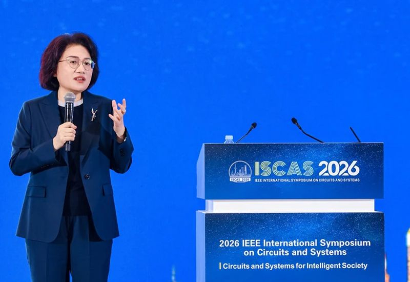
Image source: Huawei Technologies Co., Ltd.
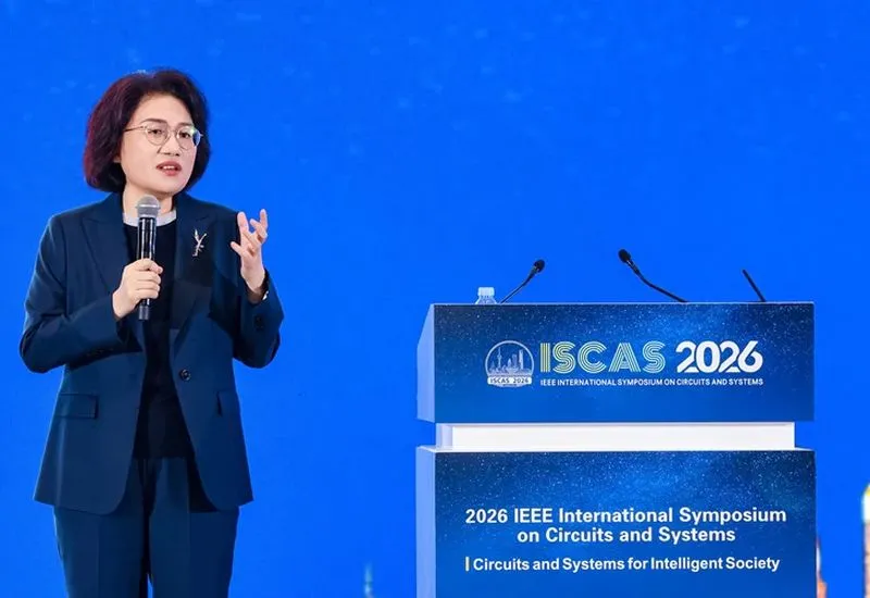
as mentioned before TrendForce Referring to the Global Times, the author of the new publication is He Tingbo (pictured above), one of the ideological inspirations for the transition to the new layout method. According to reports, when building the Kirin 2026 chip, the transistor density can be increased by 55%, and the power consumption level of many key modules has been reduced. Indeed, the performance level remains the same, there is an important nuance here.
As the source explained, the principle of “tau scaling” is time-related because it improves performance by reducing the number of paths data must take within the chip. If you increase the clock frequency, power consumption will increase, and so will heat dissipation. It is quite difficult to combat the latter in “multi-layer” chips, which are obtained by “adding” planar structures to two layers, and in the coming years this factor will become a significant limitation on Huawei’s ability to improve chip performance. This is emphasized in the title section of the Huawei report, which asks whether the company’s new chips should melt down.
Since Huawei did not increase the clock frequency of the chip, Kirin’s NPU power consumption was reduced by 66%, GPU power consumption was reduced by 58%, and CPU power consumption was reduced by 41%, and the performance is equivalent to the previous generation product. In the mobile world, this is a pretty important result, as it can extend the battery life of your device. In particular, the NPU neural unit showed a performance of 29 TOPS when the operating frequency was 63% lower than the previous generation model, the voltage was reduced from 0.85 V to 0.55 V, and the energy flux density was reduced by 73%.
A Huawei representative stated that the main benefit in energy consumption is achieved by reducing the cost of mobile data, rather than by performing the calculation itself. If we consider that the energy consumption of type 1 as part of the “system on a single chip” amounts to 80% of the total energy consumption, the resulting savings are significant from a practical point of view. New methods of chip layout can reduce data transmission paths within the chip by 20% to 70%. The blocks within the wafer are distributed in two layers and connected to each other by vertical channels with a spacing of 1.5 microns. As part of Kirin 2026, there are approximately 50 million such vertical interconnects, of which 10% to 15% are used for signal transmission.
Kirin 2027 samples have shown a reduction in vertical channel spacing to 1 micron, while their number increases to over 100 million. In the next three years, Huawei expects to reduce the channel pitch to 720 nanometers and increase the number of channels to more than 200 million. As pointed out in the Huawei publication, if all the gain in signal transmission time is used to increase the clock speed of the chip, then power consumption will inevitably increase. In addition, the new design method requires changes to many production processes, which is an expensive and time-consuming process. On the other hand, in the context of tense cooperation with the West, China’s Huawei cannot boast of having chosen an alternative technological development path.
If you find an error, select it with your mouse and press CTRL+ENTER.