


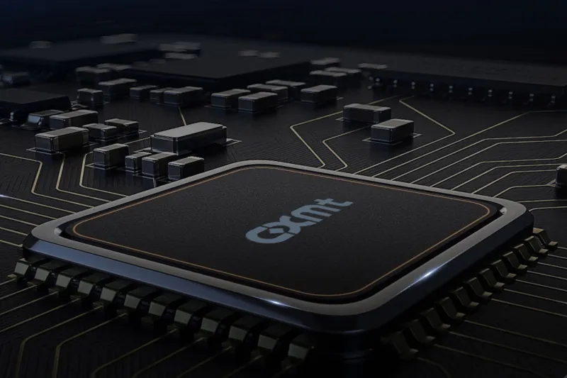
Changxin Storage, China’s largest RAM manufacturer, has begun trial production of HBM3E memory stacks, but success will not be easy in the short term. According to Korean media reports, the yield rate of Changxin Storage does not exceed 25%, and in the semiconductor industry, the gold standard for mass production is 80% North Korea.
Image source: cxmt.com
SK hynix is considered the global leader in HBM3 (and accelerated HBM3E) and currently has a product yield of 90% since starting mass production of these products in 2022. Experts say the main reason for CXMT’s failure was the difficulty in mastering the through-silicon via (TSV) technology required for vertical alignment of DRAM layers. The eight-layer layout HBM3E product suitable for Chinese companies has a yield rate of about 30% in the front-end stage, that is, the preparation of components; only 70% of the wafers that pass this stage are considered suitable products for the back-end stage. In short, of the 100 HBM3E units put into production, nearly 80 failed final testing.
Changxin Storage is supplying low-volume HBM3E images to Chinese companies such as T-Head (owned by Alibaba) and Cambrian, and continues to work hard to improve yields. The problem is not the production technology of the DRAM crystal itself – Changxin Storage’s standard DRAM chips produced using G4 process technology (17nm level) have not been subject to serious complaints. But DRAM wafers designed to run in HBM have higher surface areas and must meet more stringent specifications than standard products. Experts interviewed by North Korea said it is much more difficult to ensure that such products meet quality standards, even if they follow the same production process. If Changxin Memory can ensure sufficient quality of standard DRAM production, difficulties will arise at the level of converting it to HBM.
Chinese manufacturers have encountered difficulties in mastering TSV technology. These are microscopic copper interconnects that run vertically through the DRAM layers to carry electrical signals. This requires thinning a single DRAM platter to tens of microns, drilling thousands of tiny holes in the silicon, and filling them with copper. Even a displaced or incorrectly filled hole can cause defects, making this process one of the most difficult in semiconductor production.
I believe that in this field, the technical gap between Changxin Storage and leading manufacturers is the largest. Samsung’s HBM2 chip has more than 5,000 TSV connections per chip, SK Hynix’s HBM3 has more than 8,000, and Changxin Storage’s number is about 3,000. By lowering this number, Changxin Memory sacrifices throughput to reduce manufacturing complexity, but the yield is still lower than Samsung and SK Hynix. As early as 2024, SK Hynix admitted that its TSV product yield rate was between 40-60%.
Loss in product yield also occurs during the finishing stage (backend), which involves the mechanical arrangement of the crystals on top of each other and their interconnection. If at least one of them shifts, microscopic air bubbles may form in the joint area, or the layers may deform under the influence of thermal compression – as a result, the entire multilayer structure is discarded. As the number of layers increases, the number of possible failure points will also increase, and production will become more complex; that is, when moving from an 8-layer layout to a 12-layer layout, the difficulties of Changxin storage will become disproportionately greater.
From this, experts concluded that TSV technology can only be stabilized in practice after accumulating many years of experience. The Chinese company has quickly closed the gap in DRAM production technology, but doing so for TSV in the shortest possible time will be very difficult. Samsung, on the other hand, improved its HBM4 product yield from less than 60% to 80% in just six months; therefore, it is too early to draw any conclusions about CXMT’s 20-25%.
If you find an error, select it with your mouse and press CTRL+ENTER.