
SemiAnalysis conducted a detailed analysis of Intel’s Panther Lake processors, providing the first independent examination of the chip’s design and Intel’s most advanced process technology to date. Experts focused on Intel’s 18A production technology, which includes two key innovations – the new RibbonFET transistor and the PowerVia power supply system.
Image source: Intel
In short, the main conclusion of the study is that Intel can indeed implement both technologies into production consumer processors. However, the analysis results show that in terms of logic component density, Intel 18A roughly corresponds to TSMC’s N3E process technology. At the same time, the designations 18A and N3E should not be taken as designations for the transistors’ physical dimensions of 1.8 and 3 nanometers respectively: these are simply marketing names for technical standards.

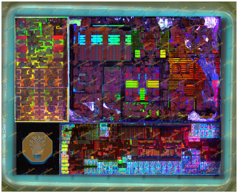
Snapshot of all Panther Lake processor chips
Panther Lake is Intel’s first consumer processor to use RibbonFET transistors, an implementation of its proprietary gate-all-around (GAA) technology. In traditional FinFET transistors, current flows through vertical silicon “fins.” RibbonFET uses four stacked horizontal silicon nanosheets. Gates surround them from all sides, allowing more precise control of the flow of current and reducing leakage.

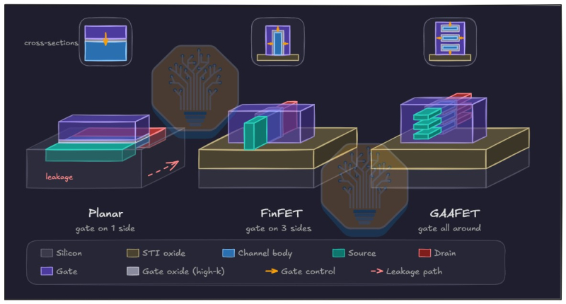
Interestingly, Intel uses four nanochips in a transistor, while Samsung uses three nanochips in its SF2 process. Meanwhile, on Samsung, the layers are significantly wider, so the final density depends not only on their number, but also on the geometry of each layer.

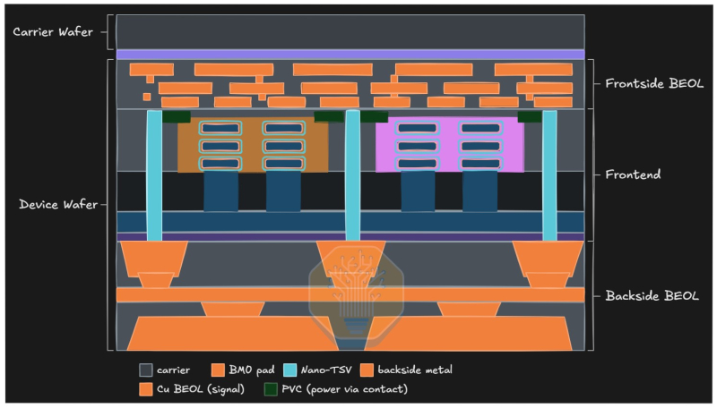
The second key innovation is PowerVia, a backside power supply system made by Intel. In traditional chip designs, power and signals pass through metal layers above the transistors. PowerVia moves most of the power infrastructure to the backside of the die, beneath the transistor layer. This frees up the top metal layer for signal connections and allows for shorter, wider power paths, potentially lowering resistance and improving voltage stability in the most demanding parts of the processor.
However, this approach also comes with compromises. Moving the power infrastructure to the backside of the die increases technical complexity, along with additional parasitic capacitance and thermal resistance. Therefore, the advantages of PowerVia must be considered in conjunction with the cost of the new technology.
In this case, the most interesting disassembly results concern the density of the transistors. SemiAnalysis measured the transistor density of Panther Lake logic on Intel 18A and found that it is roughly the same as the transistor density of TSMC N3E GPU logic. This is a major achievement for Intel, which has lagged behind TSMC in advanced process development in recent years. However, according to SemiAnalysis’s assessment, the maximum density of 18A does not exceed the newer TSMC N3P and N2 standards and Samsung SF2.
More detailed measurements show that based on representative logic cell models, 18A is approximately 18.6% denser than Intel 3 and roughly at the same level as TSMC N3E. At the same time, the researchers stress that this is a comparison of a single unit, not an entire area of the crystal: the actual density depends on the collection of processor blocks and their placement.

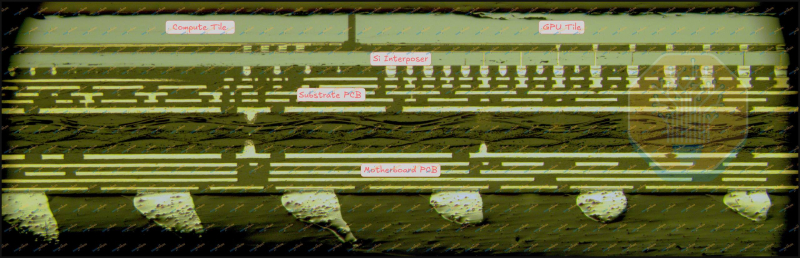
Cross-section of Panther Lake: Compute and graphics modules mounted on silicon interposer
The segment also shows how Intel is using small die architecture and advanced packaging to combine components made using different manufacturing processes. Panther Lake uses Foveros-S packaging technology to place independent computing, graphics and I/O chips on a passive silicon substrate. The computing crystal is manufactured using Intel 18A technology. There are two versions of the graphics part: the quad-core Xe3 chip is made by Intel 3, while the larger version with 12 Xe3 cores is made by TSMC using N3E process technology. The I/O chips are also manufactured by TSMC using the older N6 process.

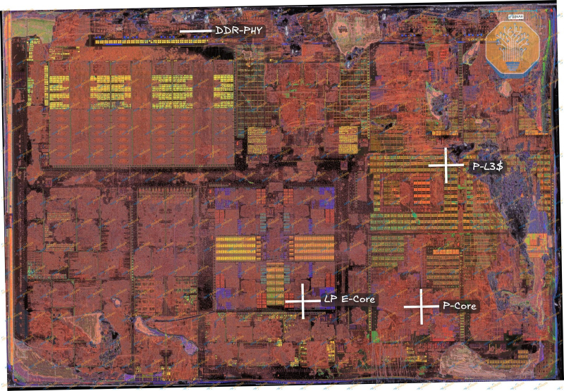
However, the design of Panther Lake is significantly different from Meteor Lake and Arrow Lake. Now, the NPU, energy-saving LP E core, memory controller, PHY, multimedia and display units are located directly on the computing chip. This can reduce the number of die-to-die connections, although some front-end and analog logic must now be placed on the more expensive 18A process technology. Instead, separate I/O crystals are responsible for external interfaces – specifically PCIe and Thunderbolt. It is produced using TSMC’s more mature N6 process technology, eliminating the need to move these relatively slow interface blocks to the expensive Intel 18A.

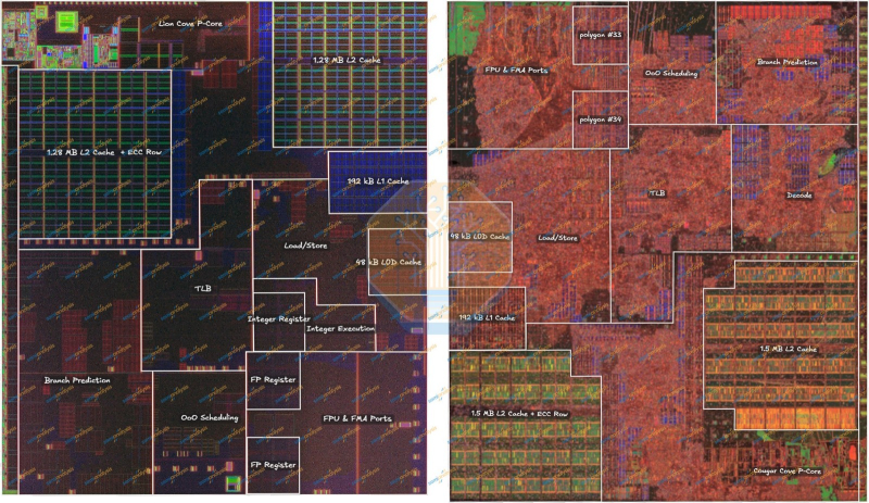
On the left is the core of Lions Cove in Moon Lake, and on the right is Cougar Cove in Panther Lake
SemiAnalysis also noted architectural changes to the processor. The Panther Lake CPU architecture is an evolution of the previous generation, not an entirely new development. Cougar Cove’s performance core area is close to Lunar Lake’s Lion Cove, but the secondary cache size increases from 2.5 MB to 3 MB per core. According to experts, Cougar Cove allows you to place about 20% more secondary caches for the same core area. At the same time, the total amount of level 3 cache in the performance core decreased by approximately 14.8%. And the energy-efficient Darkmont LP core’s quad-core cluster is about 5 percent smaller than its predecessor.

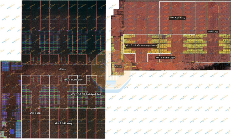
The Intel NPU 4 in Lunar Lake processors (left) is larger than the NPU 5 in Intel Panther Lake processors (right)
Neural Accelerator has been significantly redesigned. According to SemiAnalysis data, Panther Lake’s NPU 5 occupies 36.9% less area than Lunar Lake’s NPU 4, while maintaining comparable INT8 computing performance. Intel consolidated computing units into fewer, larger neural cores while reducing the number of Scratchpad and DSP SHAVE native memory units from 12 to 6. In addition, NPU 5 gains hardware support for FP8, a lower-precision data format increasingly used for inference on AI models.

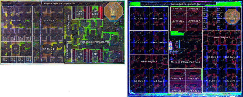
Two options for Intel Xe3 graphics cards in Panther Lake: the Intel 3-based GT1 chip on the left, and the N3E-based GT2 on the right
The graphical component also provides an interesting comparison. The single Xe3 core in the Intel 3-based GT1 graphics chip is about 55% larger than the cores in the 12-core TSMC N3E-based GT2 chip. Additionally, the Xe3 cores on Intel 3 are about 69% faster than the equivalent cores in Lunar Lake. In other words, Intel has the ability to produce GPUs using its own process technology, but TSMC N3E allows more graphics processing units to be placed on the same silicon area.
Judging from the analysis results of Panther Lake, it cannot be said that Intel has regained unconditional technology leadership. However, it shows that the company is able to simultaneously introduce two important technologies into a range of consumer products – RibbonFET and PowerVia. At the same time, 18A shows a density level comparable to TSMC N3E, but has not yet surpassed competitors’ newer processes in this indicator. Intel’s 18A’s ultimate competitiveness will depend not only on transistor density, but also on a combination of performance, power efficiency, wafer yield, and manufacturing cost.
If you find an error, select it with your mouse and press CTRL+ENTER.