
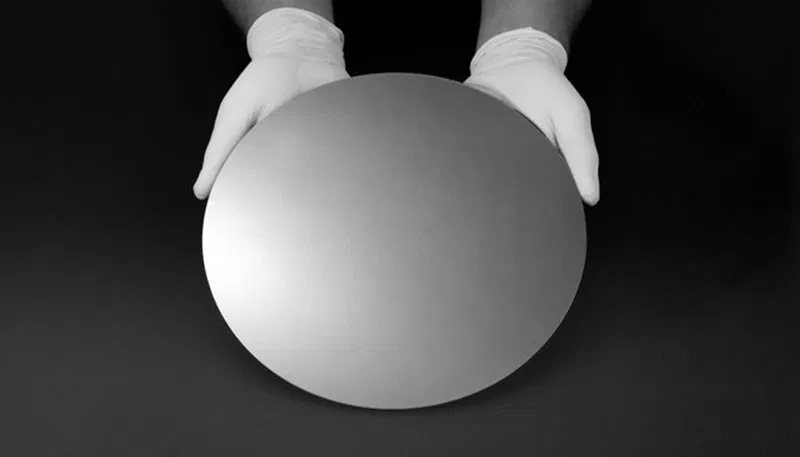
San Francisco-based Diamond Foundry announced the production of the world’s first single-crystal diamond wafer with a diameter of 200 mm (8 inches). Such diamonds do not exist in nature on Earth, and production for a long time stalled on plates with a diameter of no more than a couple of inches. Meanwhile, diamond is necessary for electronics with the highest performance parameters.

Image Source: Diamond Foundry
Diamond has high thermal conductivity, a multiple of that of copper, a wide bandgap, which allows operation at temperatures prohibitive for semiconductors and in conditions of strong electromagnetic fields, as well as high resistance to breakdown. Everything taken together makes diamond indispensable for the transition to the next stage of electronics development, at least power.
Company emphasizesthat the resulting sample is a single continuous single crystal, and not a combination of several diamond segments and not a polycrystalline material. Its diameter is 200 mm – about the same as standard silicon wafers used in many semiconductor industry plants.
According to Diamond Foundry, the achievement required improvements in plasma generation techniques, crystal growth chemistry, reactor design, thermal management, metrology and manufacturing control. Work on scaling the technology lasted about 25 years. The company especially acknowledges the personal contributions of experts such as Stefan Gsell and Martin Fischer, who have been working on this problem since before joining Diamond Foundry in 2022.
“This is one of those milestones that once seemed almost unattainable,” said Martin Roscheisen, CEO of Diamond Foundry. “Hundreds of Diamond Foundry engineers, scientists and technicians contributed to helping us achieve this.” It is the result of countless experiments, failures, inventions, machine modifications and discoveries made over more than ten years.” It is very significant that the announcement was made during a speech by the head of Diamond Foundry at the CarbonSemi 2026 conference in Ningbo, China, which is taking place these days.
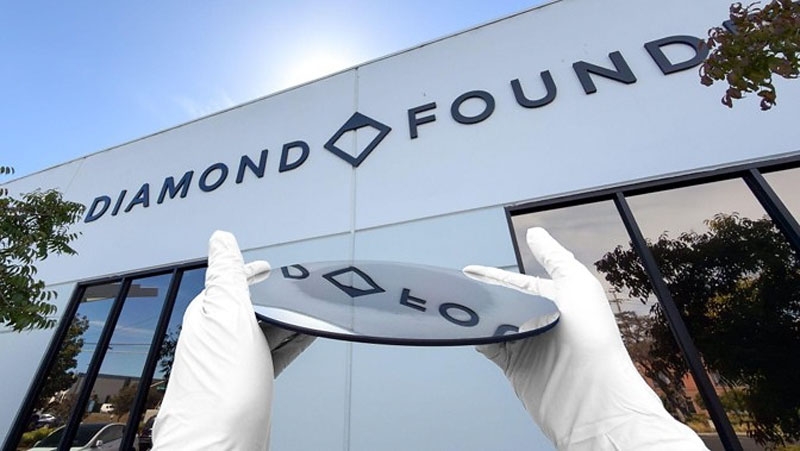
In addition to being used as power electronics or high-temperature chips that can even withstand operation on the surface of Venus, where lead flows like water, diamond is being considered and already used as a material for substrates and heat sinks in high-power semiconductor devices, artificial intelligence accelerators and high-performance computing systems. In particular, diamond can help remove heat from local hot spots on chips, where high heat flux densities create severe cooling limitations.
In his report, the head of Diamond Foundry did not provide specific data on the level of defects and the productivity of lines for growing single-crystal diamond wafers with a diameter of 200 mm. We are waiting for more detailed data on this matter.
If you notice an error, select it with the mouse and press CTRL+ENTER.