

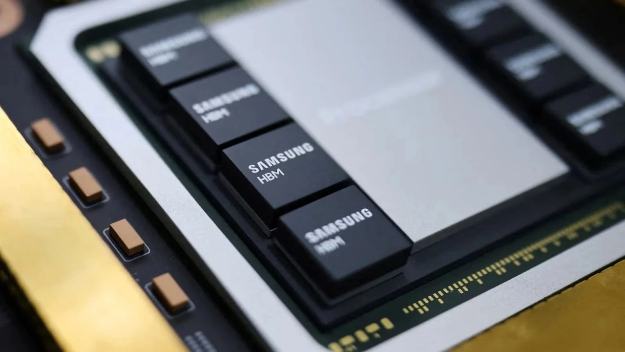

Samsung presented a new concept developed by HBM on Hot Chips, in which the basic memory crystal is no longer just a connecting link. The company hopes to turn it into a mature computing component for future artificial intelligence accelerators.
Current HBMs are based on two types of crystals: the core chip with DRAM cells and the base chip responsible for memory management and communication with the GPU or other accelerators. However, throughput growth is increasingly limited by TSV, number of interfaces, and power consumption. Therefore, Samsung intends to move Base Die to a more modern technological process and expand its capabilities.
The company describes a three-stage path to achieve this goal: first it plans to clear space and add new features, then move to custom HBM and advanced HBM, and the last point will be ZHBM with a full 3D layout. In such an architecture, DRAM will be placed directly on the computing logic, which will significantly reduce the data transmission path.