

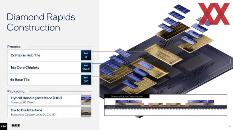
Intel spoke at the Hot Chips conference about the Diamond Rapids series of Xeon processors that will be available next year. These will be the first Intel processors produced using advanced Intel 18A-P processing technology. The company has reportedly revealed details of the new chip architecture Hardware luxury.
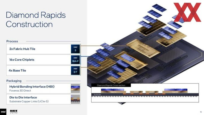
Image source: hardwareluxx.de
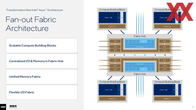
In the center of the processor assembly are two I/O memory hub (IMH Tile) small chips, which are manufactured using Intel 3 process technology and are responsible for the operation of the memory and I/O subsystems. There are also up to four Base Tile chips made using Intel 3-T technology. In addition, each of them contains an LLC last level cache (Last Level Cache), which is common to multiple Core Tile computing chips. The Core Tile itself contains processor cores with L1 and L2 caches, and these small dies are produced using Intel 18A-P technology.
To connect the Core Tile to the Base Tile, Intel uses Hybrid Bonding Interface (HBI) technology, which the company calls Foveros 3D Direct. For communication between IMH and Base Tile chiplets, a D2D (Die-to-Die) inter-die interface based on UCIe-S (substrate copper link) is used.
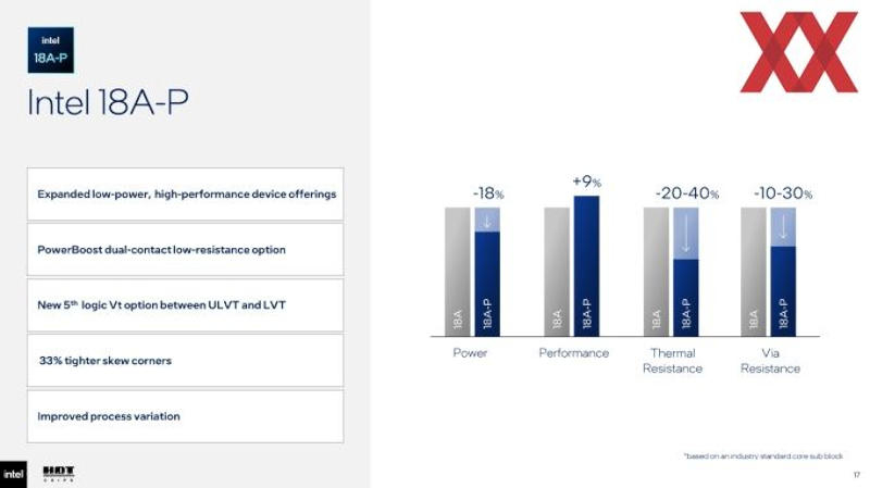
Intel 18A-P is an evolution of Intel 18A process technology, providing higher performance and additional transistor optimization options for performance and power consumption. For high-performance transistors, Intel provides two power pins on the back of the die. In addition, a fifth pair of threshold voltage (Vt) options has appeared, located between LVT (low voltage) and ULVT (ultra-low voltage), extending the ability to optimize transistor performance and power consumption.
Intel claims that the 18A-P process reduces performance differences by 33% between extreme PVT (process, voltage, temperature) scenarios that take into account process variations, supply voltage, and operating temperature. As a result, transistor parameters become more uniform both within the same board and between individual crystals. Therefore, when designing, you can include smaller margins in clock frequency, voltage, and timing, which allows you to increase frequency and energy efficiency, and increase yields of suitable products.
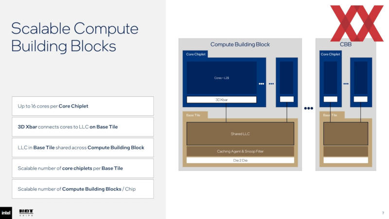
Up to 16 Core Tile computing dies interact with two central IMH dies. Each Core Tile contains 16 processor cores and has its own L2 cache, bringing the maximum number of Diamond Rapids cores to 256. The last level cache is located in the Base Tile and can be accessed through the 3D Xbar of its associated Core Tile. Its total capacity can reach 1280MB, and each of the four Base Tiles is 320MB.
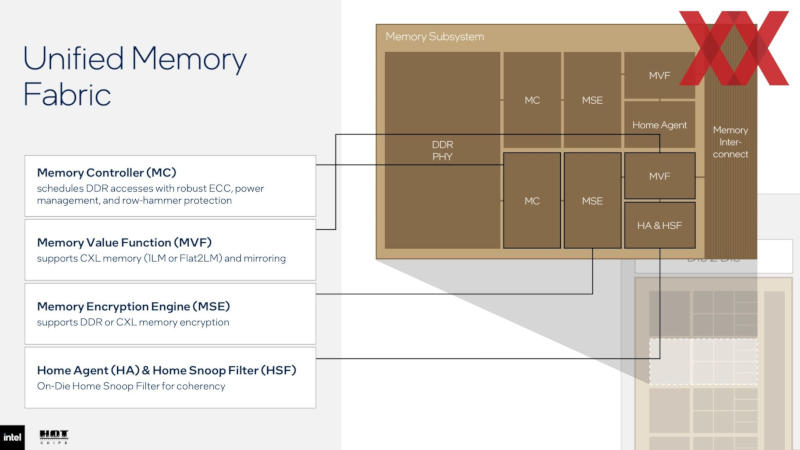
Each IMH Tile chiplet contains six PHYs for D2D interfaces, as well as unified memory architecture subsystem components. It includes PHY DDR, memory controller, Snoop filter, and memory encryption and decryption accelerator. The I/O subsystem contains four sets of high-speed lanes that can be used for PCI Express, CXL, or UPI in multi-slot connections. Diamond Rapids will support DDR5-12800, total memory bandwidth up to 1.6 TB/s, and up to 128 PCI Express lanes.
Diamond Rapids processors will also receive support for Advanced Matrix Extensions (AMX) and AVX 10.2 instructions, QAT, DSA and IAA hardware accelerators. The architecture includes branched fan-out structures and modular CBB (Compute/Building Block) compute blocks using Foveros 3D direct and Hybrid Bonding Interconnect (HBI) connections. Additionally, there are Intel TDX and SGX security technologies, improved RAS (reliability, availability, serviceability) and QoS capabilities, and telemetry tools.
If you find an error, select it with your mouse and press CTRL+ENTER.