
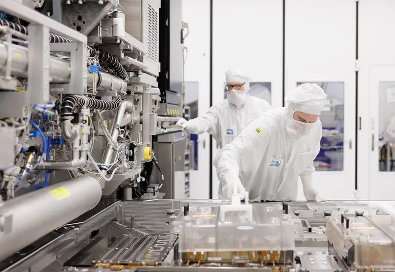
So far, it is believed that TSMC, the largest contract chipmaker, is in no hurry to master high numerical aperture EUV lithography equipment because it is still extremely expensive. However, at the turn of this decade and the next, TSMC will join Intel and Samsung in this area and also participate in the migration to new standard size photomasks.
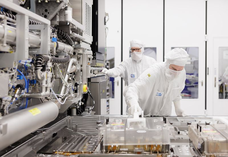
Image source: ASML
Photolithography involves using a photomask to outline the future microcircuit and projecting it onto a semiconductor crystal so that chemical etching can be used to further form the microstructure. Historically, this was done using 150mm photomasks, but the semiconductor industry is now looking to double the size to increase factory productivity and reduce costs.
As with high numerical aperture EUV equipment, migration to new photomask sizes is considered difficult and expensive, but a joint effort by all major wafer manufacturers will help reduce associated costs, as explained Bloomberg. Marco Pieters, technical director at ASML Netherlands, explained that the throughput of high-NA EUV-level scanners can be increased by 40% and the wafer design process will be simplified due to the transition to 300mm photomasks.
Sources say Samsung and TSMC will start using High-NA EUV equipment in wafer mass production: starting in 2028 in the first case and 2030 in the second case. Intel has moved away from experimentation in this area to selectively using the device to mass-produce its Panther Lake processors with Intel 18A technology. For ASML, which supplies such scanners, the road is even longer, as the company launched a low numerical aperture EUV device as early as 2019 before starting to prepare to bring a high numerical aperture system to the market.
However, it should be recognized that starting in 2030, TSMC will combine high numerical aperture EUV equipment with traditional 150mm photomasks. A pilot line to produce larger 300mm photomasks will start in 2031, with mass production for wafers not expected to begin until 2033.
As noted in a company statement, Samsung will begin producing memory using high numerical aperture EUV equipment in 2028 and will work with “industry partners” to transition to new standard size photomasks. Intel added that it has been pushing the idea of moving to larger photomasks for more than three years. This migration will allow the industry to create more productive and advanced semiconductor wafers.
If you find an error, select it with your mouse and press CTRL+ENTER.