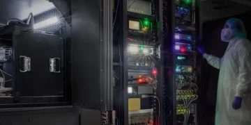


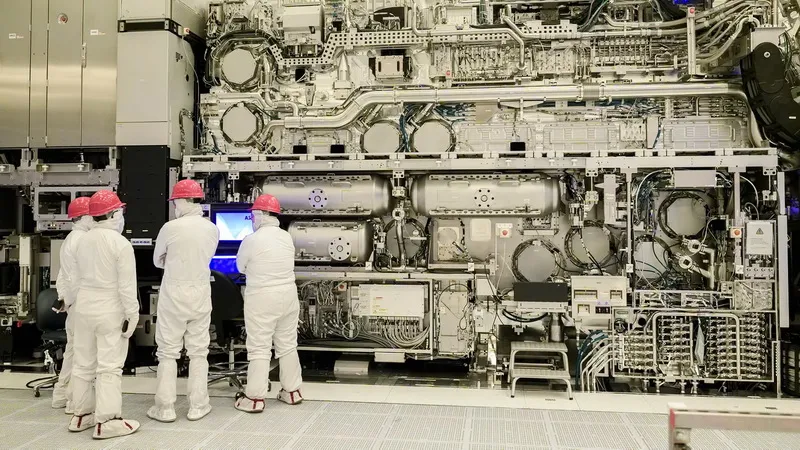
Intel said it has processed 1 million 300mm silicon wafers using extreme ultraviolet (EUV) high numerical aperture (High-NA) lithography. The use of high numerical aperture EUV in silicon wafer manufacturing poses many challenges due to increased process complexity.
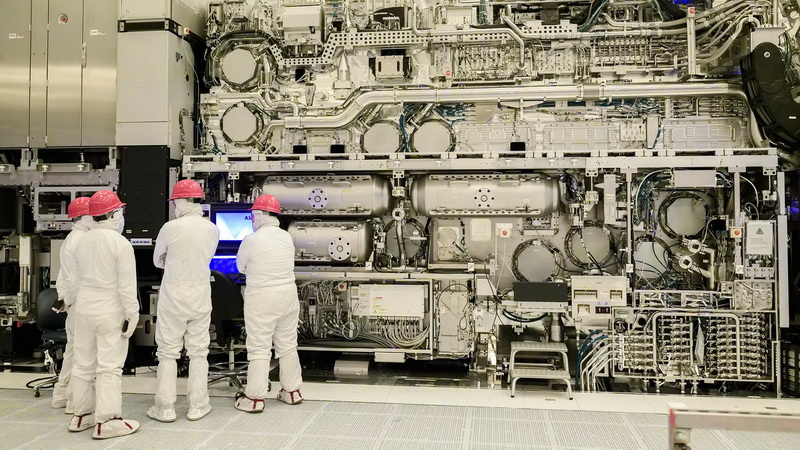
Image source: Intel
In 2024, Intel installed the ASML TWINSCAN EXE:5000 High-NA EUV system for 14A process research and testing. However, Intel has since found more efficient ways to use High-NA tools outside of the 14A regulations, extending its use to the 18A regulations.
For some Panther Lake processor die models, Intel uses high NA exposure to stack multiple layers of silicon instead of relying solely on low NA. Additionally, Intel offers this high numerical aperture configuration to external customers because it benefits them as well. Intel collaborated with ASML to complete acceptance testing of 14A process technology at Intel foundries to improve silicon wafer production efficiency. The scanner used for this operation is the TWINSCAN EXE:5200B, the second version of Intel’s ASML high numerical aperture EUV scanner after the TWINSCAN EXE:5000 originally used for pilot 14A. Intel previously reported that it processed more than 30,000 wafers in a single quarter, simplifying the manufacturing process and significantly speeding up the production cycle by reducing the steps required to process a single layer from 40 to less than 10.
Currently, Intel remains the only company actively using high numerical aperture EUV lithography technology to produce semiconductors. TSMC said it can maintain a competitive advantage by leveraging existing low numerical aperture EUV lithography technology, reducing process size and improving it with each product generation.
According to reports, Samsung foundry will postpone the introduction of EUV high numerical aperture lithography technology in the 1nm process until 2030, which leaves the entire industry still several years away from adopting high numerical aperture lithography technology. Low numerical aperture equipment is half the cost of advanced high numerical aperture EUV systems. ASML’s state-of-the-art high numerical aperture EUV system costs approximately $400 million, making it extremely expensive even for a modern semiconductor foundry.
If you find an error, select it with your mouse and press CTRL+ENTER.