


Scientist at ETH Zurich developed Technology that uses wafer production methods to produce micro OLED pixels. The new method makes it possible to create organic light-emitting structures using photolithography, the same process used to make microcircuits. This development paves the way for the creation of ultra-small displays for augmented reality devices and more.
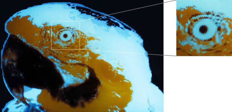
Image source: ETH Zurich
The main problem with OLED miniaturization is the incompatibility of organic light-emitting materials with traditional photolithography. In the fabrication of microcircuits, photolithography uses corrosive solvents and chemicals that can damage organic molecules. Conditioned organisms – organic compounds – cannot withstand the harsh chemical reactions involved in semiconductor production.
To this end, Swiss scientists have created a new light-emitting polymer that has the properties of both an OLED material and a photoresist. Once applied to the wafer surface, these compounds can change structure under the influence of UV radiation to form microscopic light-emitting elements of a given shape. In other words, UV light can be used to paint OLED pixels of a given size and shape, creating the entire pixel array of a microdisplay.
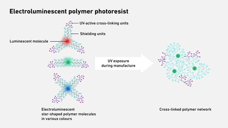
The key development decision is the molecular structure of the OLED material based on the “core-shell” principle. In the center of this molecule there is an organic component responsible for radiation of a certain color, and around it there is a star-shaped chain with sites for chemical reactions. When exposed to UV light, the outer parts of the molecule are stitched together, turning the exposed areas into a solid structure. At the same time, the protective inner layer protects the luminescent core from chemical exposure during processing.
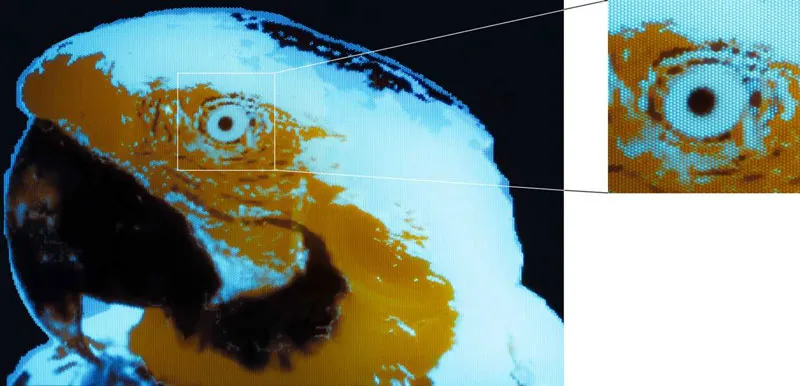
To demonstrate the technology, the researchers created several test samples. One is a color fluorescent image of a macaw, measuring only 300 × 430 microns and composed of 250 × 350 pixels. To date, this is the highest-resolution image of any multicolor structure created using photolithography, and is comparable in size to the simplest microorganisms.
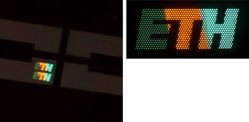
In addition, the team created a miniature illuminated ETH Zurich logo with dimensions of 1 x 2.4 mm based on electronically controlled LED components – this is already a prototype of a real display, with the parrot image triggered by external illumination. The next steps will be to further reduce pixel size and integrate control electronics to create full-fledged microdisplays. In addition to screens, the technology could also find applications in biomedical systems and microscopes, which require ultra-small light sources to precisely control single cells or neurons.
If you find an error, select it with your mouse and press CTRL+ENTER.