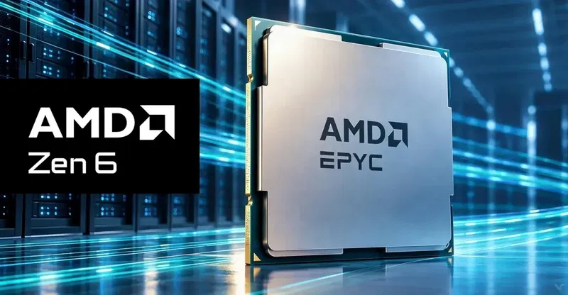
AMD has revealed additional technical details about the Zen 6 and Zen 6c architectures that power the sixth generation EPYC 9006 Venice processors. The new processors are designed to compete with Nvidia Vera and Intel Granite Rapids-AP chips. The Tom’s Hardware portal conducted the first independent tests of the new processors.
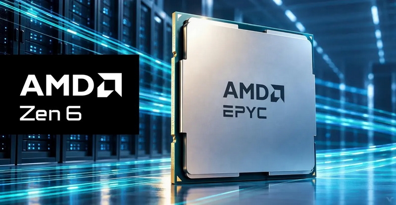
Image Source: AMD
For the production of computing chips (CCD) on the Zen 6 and Zen 6c architectures, the advanced 2-nm TSMC N2P process technology is used. Compared to N3E (used in Zen 5), it provides either an 18% increase in frequency at the same power consumption, or a 36% reduction in power consumption at the same speed.
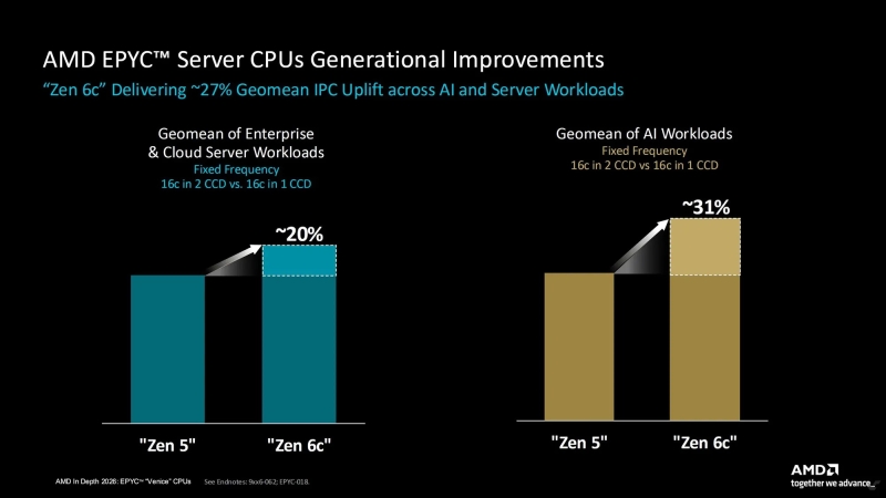
The Zen 6 design allowed the number of cores on a single chip to be increased by 50%. Standard CCD Zen 6 now accommodates up to 12 cores (48 MB L3 cache). At the same time, despite increasing the number of cores to 12 on the CCD, AMD engineers managed to maintain the latency of accessing the L3 cache at the same level – only 13 cycles, as in Zen 5. The introduction of changes made it possible to declare an increase in the geometric average IPC (the number of instructions executed per clock) in AI tasks and server loads by 27%. The maximum frequency of Zen 6 processors has increased to 5.3 GHz (versus 5.0 GHz for Zen 5).
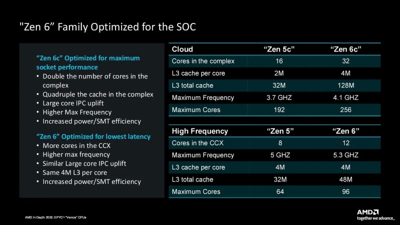
For chiplets based on energy-efficient Zen 6c cores, the largest jump in density is announced. Now one such crystal can accommodate up to 32 cores (twice as many as in Zen 5c). AMD doubled the L3 cache per core in Zen 6c (to 4 MB), which is why the total cache per chiplet quadrupled to 128 MB, and the maximum clock speed rose to 4.1 GHz (versus 3.7 GHz for Zen 5c). It’s important to note that Zen 6 and Zen 6c use exactly the same microarchitecture inside the core. Unlike Intel’s E-cores, which are based on a separate architecture and lack support for many P-core instructions, Zen 6c is simply an area-optimized design of the standard core with lower power consumption and lower frequencies.
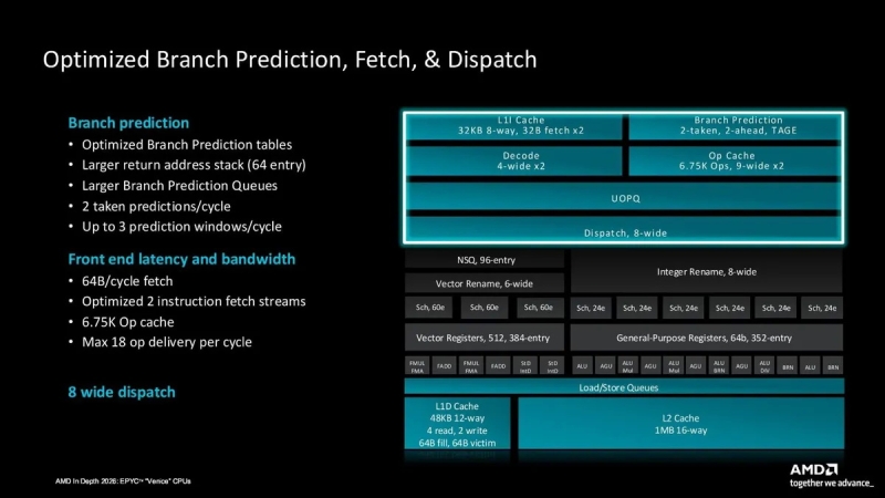
As part of the new architectures Zen 6 and Zen 6c, separate integer schedulers have been introduced and the physical register file has been expanded to 352 entries. The vector computing unit received native support for half-precision FP16 instructions while maintaining full backward compatibility with AVX-512, and FP data download throughput increased to two 512-bit or four 256-bit downloads per clock. The operation cache increased from 6 thousand to 6.75 thousand entries, and the feed throughput increased from 12 to 18 operations per cycle.
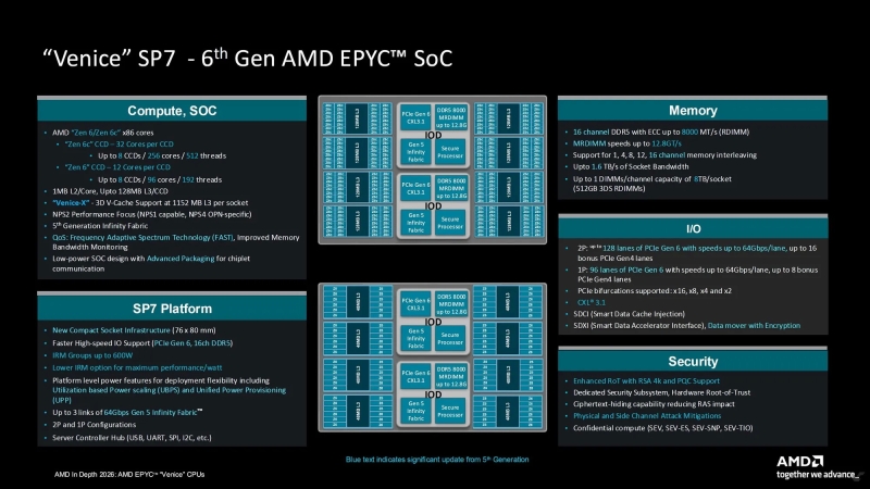
Zen 6 server processors for the SP7 socket are characterized by the presence of two input-output crystals (IODs) instead of one, located in the center of the chip, which made it possible to implement support for 16-channel RAM. It is claimed to work with MRDIMM memory modules in a 1DPC configuration with data transfer rates of up to 12,800 MT/s (with RDIMMs, speeds of up to 8,000 MT/s are supported), which provides peak throughput of up to 1.6 TB/s per socket (up to 1 TB/s when using RDIMM). The platform supports installation of up to 8 TB of memory per socket.
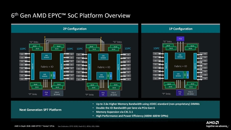
For systems with SP7, support for the PCIe 6.0 interface is also announced at speeds of up to 64 Gbit/s per line. The single-processor (1P) configuration of the SP7 has access to 96 PCIe 6.0 lanes, while the dual-processor (2P) platform offers up to 128 lanes. Each configuration also comes with “bonus” PCIe 4.0 lanes – either 8 for 1P configurations or 16 for 2P.
For systems with an SP8 connector, the number of memory channels is reduced in favor of PCIe lanes. The SP8 connector has smaller dimensions – 62.5 × 80 mm, and the platform itself supports eight memory channels instead of 16 (while maintaining support for MRDIMM modules with data transfer rates of up to 12,800 MT/s). Memory bandwidth is 819 GB/s when using MRDIMMs at maximum supported speed, and 512 GB/s when using RDIMMs. SP8 chips have access to 64 PCIe 6.0 lanes per IOD (128 lanes total per socket plus 8 PCIe 4.0 lanes), and in dual-processor (2P) SP8 configurations, up to 192 PCIe 6.0 lanes and 16 additional PCIe 4.0 lanes are available. Both platforms support the CXL 3.1 standard.
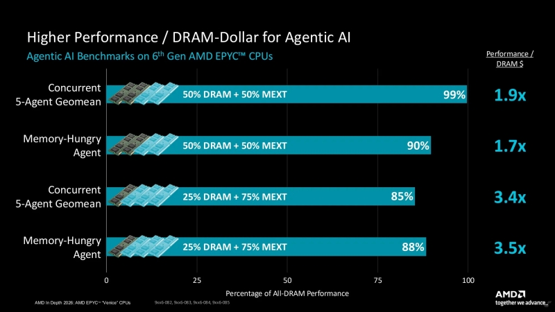
EPYC Venice will also be the first platform to support MEXT firmware technology, which uses fast flash memory as an extension of DRAM. Using AI algorithms, the system predicts memory accesses and unloads unused pages. For critical electronics design (EDA) workloads, AMD says this can retain 95% of the server’s original performance while physically reducing expensive DRAM by 50%. Even when the available memory is reduced by up to 25%, AMD claims application performance remains at 80%.
Additional architecture features and internal benchmarks from AMD can be found in the gallery below.
The Tom’s Hardware portal has two dual-processor (2P) configurations based on the SP7 socket: the 256-core EPYC 9996 (a total of 512 cores and 1024 threads per system, frequency up to 4.1 GHz) and the 96-core EPYC 9686F (384 threads per system, frequency up to 5.0 GHz).
In SPEC CPU 2026 tests for integer multi-threaded throughput (intrate), the dual-processor system on EPYC 9996, due to Zen 6 optimizations and a huge pool of threads, outperformed the previous flagship EPYC 9965 (Zen 5) by 93%. The frequency-optimized EPYC 9686F was 19% faster than the previous generation 128-core chip EPYC 9755 and 17% faster than the Nvidia Vera processor.
In floating point tests (fprate), the Zen 6 architecture demonstrated a twofold advantage over Zen 5, and the Epyc 9686F outperformed Nvidia Vera by 40%.
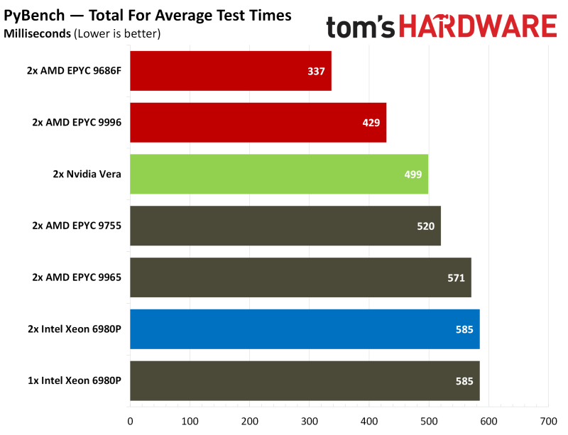
In the single-threaded PyBench test, the high-frequency flagship EPYC 9686F, due to architectural improvements and high frequency, turned out to be 32% faster than the Nvidia chip.
In the Clickhouse columnar database, the Nvidia Vera processor, due to its distributed mesh architecture, reaches peak speed faster with a “cold” cache, but after the cache warms up, the EPYC 9686F takes over the lead.
In Blender, the new EPYC 9996 completes complex scenes (like Barbershop) 35% faster than its predecessor. In code compilation tasks (LLVM, Godot, ImageMagick), Venice processors regained their undisputed first place, ahead of Arm architecture chips (Vera).
In specific HPC tasks like CloverLeaf and FFTE, the EPYC 9686F processor demonstrated almost twofold superiority over its competitor from Nvidia.
The results of other tests can be found in the Tom’s Hardware article.