



The successor to ASML’s most advanced chip technology could be available in about a decade, replacing High NA EUV with Hyper NA EUV. Engineers from a Dutch company, as well as employees of the company Carl Zeiss, which supplies optics to it, wrote about this in a peer-reviewed article.

Image source: asml.com
The new Hyper NA technology will allow the formation of chips with smaller elements. It will leverage much of the companies’ existing technology in advanced ultra-hard ultraviolet (EUV) lithography scanners, although some challenges remain to be overcome. ASML has already begun development of this installation, but a final decision on mass production has not yet been made – however, it is important for the prospects of the company itself, as well as its partners and competitors.
Hyper NA technology will continue to use the 13.5 nm EUV wavelength used in current installations, but will have an optical system with a larger numerical aperture. The new technology should provide a resolution of about 5 nm – versus 8 nm for current ASML EUV installations of the High NA class with a numerical aperture of 0.55. In other words, the new system will be able to form elements approximately 38% smaller.
In this case, we are talking specifically about the resolution of the lithographic installation, and not about the 5-nm technical process: modern names of technical processes no longer correspond directly to the physical size of the elements. For example, TSMC calls its most advanced process technology N2, and Intel calls it 18A, that is, “18 angstroms.” In a literal sense, these are 2 and 1.8 nm, respectively, but transistors manufactured to these standards do not have gates exactly 2 or 1.8 nm wide. These designations are rather the names of the generations of the technological process and reflect their position in relation to previous generations and the level of density, productivity and energy efficiency achieved. We wrote more about this here.
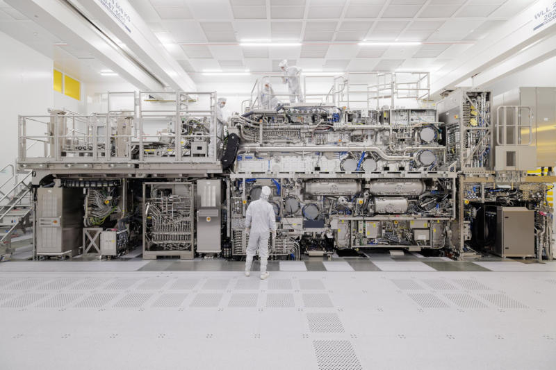
By the way, among chip manufacturers, only Intel has so far begun to use High NA equipment, specifically for the 18A process technology. TSMC and Samsung produce their 2nm chips using EUV lithography, but in the future they will also switch to High NA – Samsung in 2028, and TSMC in 2030.
Zeiss is already capable of producing mirrors with the precision required for Hyper NA – while the installation itself will be only marginally larger in size than High NA systems, which are comparable in size to a double-decker bus. To create systems superior to Hyper NA, light with even shorter wavelengths will likely be required, but this is still at the research stage.
ASML’s current light source “can be used unchanged” for Hyper NA; an alternative method using free electron lasers would not require changing the design of the lighting system, the engineers noted. These remarks are relevant for American startups: xLight is developing radiation sources based on free electron lasers – Elon Musk hinted that he might bet on them at his Terafab plant in Texas; and Substrate is involved in X-ray lithography.
If you notice an error, select it with the mouse and press CTRL+ENTER.


