American startup Architect Labs presented Frostbite, an experimental general-purpose processor architecture developed from the ground up using artificial intelligence. In benchmarks, the development completely crushed the best processor of our time, the name of which remained secret for legal reasons. Artificial intelligence has proven poised to revolutionize chip design.
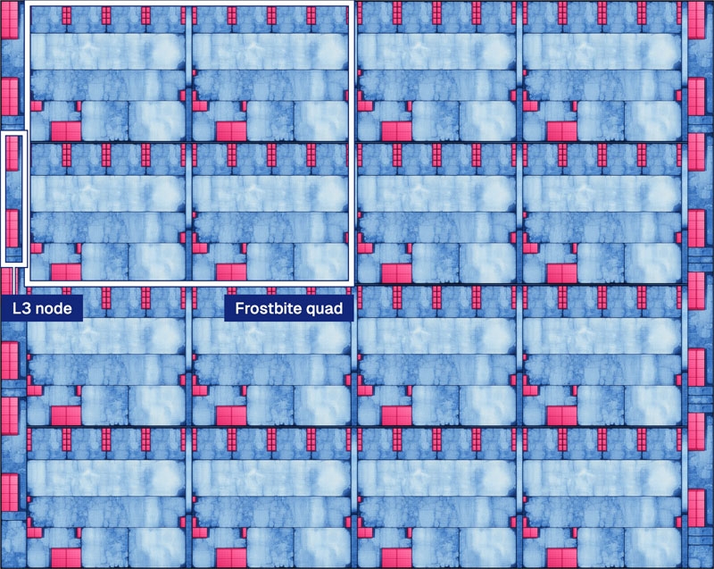
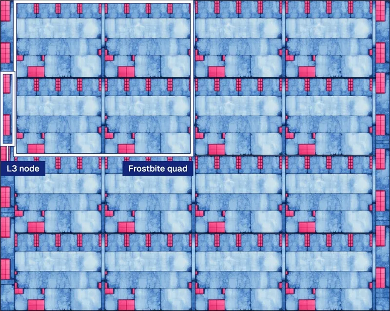
The Frostbite processor consists of four basic blocks, each of which consists of four tiles. Image source: Architect Labs
Modern general-purpose processors—the ones found in your desktops and laptops today—are inconceivable without a host of architectural crutches. But this is an urgent need dictated by continuity and the requirement to maintain the once created list of instructions, as well as the need to develop the architecture without radically breaking the developments of past decades. To say that this eats up performance and increases power consumption is to greatly understate the problem. It eats them up. A processor architecture created from scratch allows one to count on faster calculations only due to the absence of such “relics of the past.”
Artificial intelligence has just matured enough that it can be entrusted with the work of designing processor architecture. For a human team, this would require years of work, which AI is ready to cope with much faster. The same company Architect Labs in August of this year announced the development of the Redwood artificial intelligence accelerator for AI tasks in just two weeks. However, the company kept silent about how long it had been in development. Frostbite processor project.
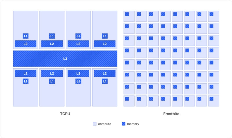
Comparison of the basic structure and cache hierarchy of a conventional multi-core CPU and a multi-core Frostbite
The main feature of Frostbite is the use of a mathematical calculation model called interaction nets (interactive networks), proposed back in 1990. Unlike traditional processors, which must determine dependencies between instructions and control their execution, Frostbite uses an explicit description of the relationships between operations. This allows independent computational tasks to be executed simultaneously without the traditional out-of-order execution mechanism. According to the developers, on 25 test tasks, the new architecture showed an average 4.59-fold advantage in performance per watt relative to the “traditional processor core” of an unnamed company.
Architect Labs emphasizes that AI makes it possible to check models and architectures that designers are not interested in simply because no one has checked them yet. Verification costs a huge amount of money and time when it comes to engineers, while artificial intelligence can quickly and at much lower cost test bold ideas, as the company demonstrated by betting on the idea of interactive networks.
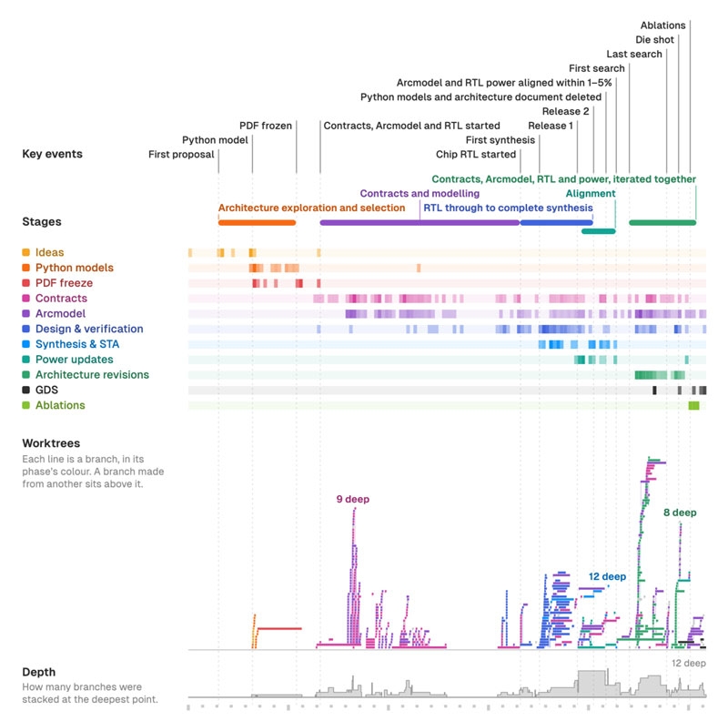
Stages of AI architecture design and implementation. as well as the work of many AI agents at each stage
The architecture is based on a concept in which a program is represented as a graph of interacting nodes. Each node has specific inputs and outputs, and computation occurs through local transformation of connected pairs of nodes. An important property of this model is that each value has a single owner and is used exactly once. This reduces the need for shared volatile memory, complex cache coherence mechanisms, and centralized thread scheduling. In addition, this approach has natural parallelism, which makes it easier to scale computing cores.
Frostbite programs are written in Vine, which has a syntax similar to Rust, and are then converted into an Ivy intermediate representation by the compiler. The processor itself consists of computational tiles that exchange tasks through the built-in network. If a block (tile) has completed its own work, it can pick up a task from a neighboring block, and if there is no work, it goes into an inactive state, saving on consumption.
Development was carried out using our own formal system for describing the architecture ASL and the Arcmodel software model. The system made it possible to automatically check the compliance of the architecture, hardware (RTL) implementations and test models with mathematically specified rules. As a result, the description of 31 hardware units was converted into more than 800 thousand lines of formal specifications.
The developers report that the Arcmodel system simulated power consumption and performance approximately 660 times faster than RTL simulation. During the optimization process, the AI considered 58 architectural changes, of which 37 were accepted. In particular, ways were found to more accurately control the clock frequency of individual blocks, which made it possible to jointly optimize the hardware and software environment. AI has shown ingenuity and resourcefulness in many ways, which has surprised people. Some of the solutions were an absolute godsend, previously not used in chip architecture.
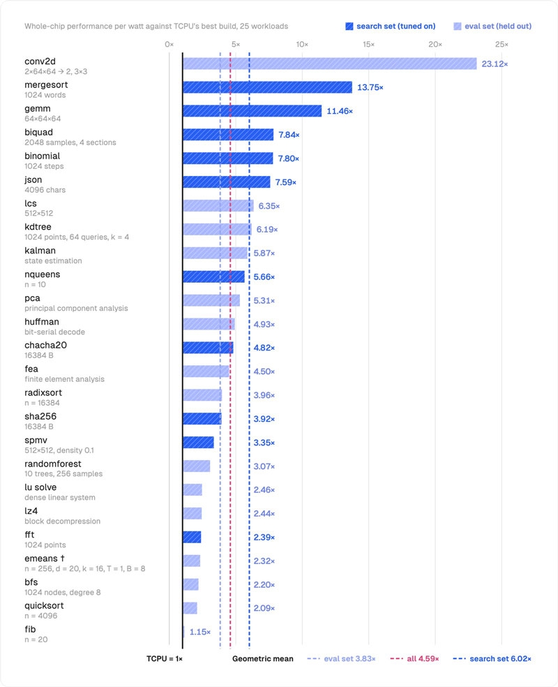
Comparison of the performance of one core of a regular CPU and one four-tile Frostbite core under different loads
Frostbite was software synthesized using 7 nm technology standards. At the synthesis stage, the calculated frequency reached 800 MHz, and in the final design of the physical topology (GDS) – 500 MHz. One Frostbite Quad computing cluster, including four blocks and four L3 nodes, occupies 0.792 mm2. For comparison, the developers used a processor core of an unknown model with an area of 0.895 mm2, also designed for the 7 nm process technology.
Based on the results of 25 tests, the average advantage of Frostbite in performance per watt was 4.59 times, and in performance per unit area – 8.77 times. On 15 tests that were not used in the initial optimization (they were first run on the processor), the energy efficiency advantage was 3.83 times. Later, the developers promise to conduct additional tests on a wider set of standard SPEC and PARSEC benchmarks.
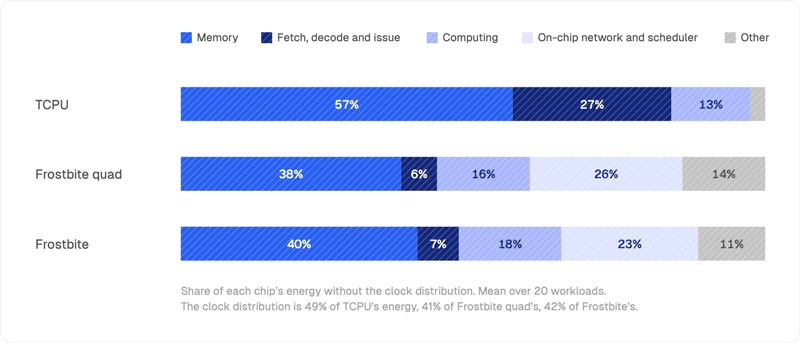
Comparison of energy consumption at different stages of working with data
The distribution of energy consumption on the graph shows how savings are achieved. Ignoring clock distribution, a general-purpose CPU spends 57% of its energy on memory operations and 27% on fetching, decoding, and issuing instructions. Frostbite reduces energy consumption for memory operations by up to 38%, and energy consumption for fetching, decoding and issuing instructions by up to 6%. At the same time, 26% of the energy is spent on the built-in network and scheduler, that is, on distributing work and transmitting messages between blocks. What’s especially noteworthy is that Frostbite’s power consumption grows approximately linearly as the number of cores scales, while for a CPU, increasing their number requires such a clutter of circuits and cache coherence mechanisms that a linear increase in power consumption is out of the question.
In the future, the developers are going to implement Frostbite on an FPGA, prepare an operating system and running programs for it, and also publish an RTL and command system.
If you notice an error, select it with the mouse and press CTRL+ENTER.