


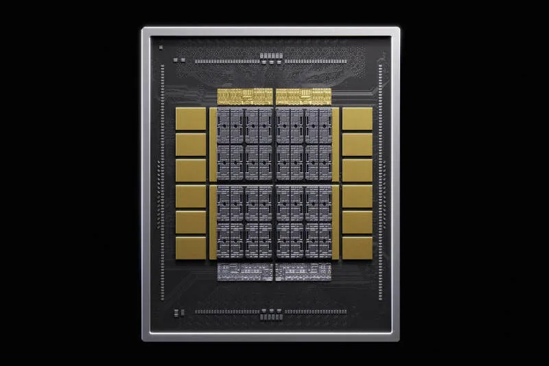
Nvidia has launched new technology as part of its NVLink Fusion initiative. NVHBM It is a customized HBM basic chip architecture specially designed for developers of their own AI accelerators. It has higher throughput, lower power consumption and saves space within the accelerator housing compared to the standard HBM4e.
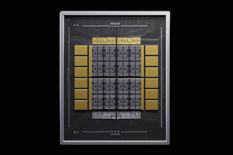
Image source: nvidia.com
As Nvidia explains, NVHBM is a customized HBM base chip designed and tested in partnership with leading memory manufacturers. Participants in the NVLink Fusion program will be able to use off-the-shelf solutions when creating their own accelerators, rather than independently developing and certifying HBM subsystems, which should reduce the time required to bring new chips to market.
NVHBM is not a replacement for HBM itself, but one of the building blocks of Nvidia’s partner-specific accelerator. One of the main advantages of this technology should be increased memory bandwidth: the company promises up to 30% more per stack compared to standard HBM4e. This will allow better loading of compute units and increase accelerator throughput for tasks where performance is limited by memory speed. In particular, faster data transfer between HBM and compute cores will increase the speed of token generation when inferring large language models.
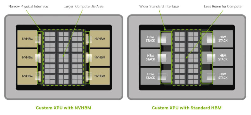
Save space with a redesigned physical memory interface. The controller has been moved from the main computing die to the base die of the 3D HBM stack, reducing the area of the PHY and associated logic by up to 67% compared to the JEDEC HBM4e standard. The narrower interface also simplifies interposer layout. As a result, developers of dedicated accelerators can gain up to 30% additional main die area for compute units and other functions.
Another benefit of NVHBM is that memory power consumption can be reduced by up to 15% compared to standard HBM4e. The released energy and thermal budget can be used to increase the accelerator’s computing power or improve sustainable performance at the same power consumption. At large data center scale, the effect becomes particularly clear: in a hypothetical 1 GW data center equipped with 2000 W accelerators, the energy savings from NVHBM would be enough to run another 15,000 XPUs, according to Nvidia’s calculations.
Improving throughput and reducing power consumption is especially important for AI accelerators that must constantly move large amounts of data, including model weights, KV caches, and launches. Nvidia claims that the combination of NVHBM and NVLink Fusion can increase the performance of a single XPU by a total of 30% due to improvements in throughput, area and power consumption.
One of Nvidia’s first partners to implement NVHBM will be Amazon-owned Annapurna Labs. The next generation of Trainium 4 accelerators will already be supported by NVLink Fusion, and the company will be able to use NVHBM in subsequent developments.
If you find an error, select it with your mouse and press CTRL+ENTER.