


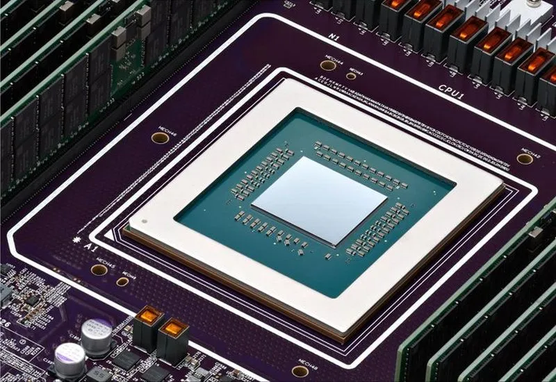
In the era before the AI boom, many developers launched new generations of processors every two years or less, but then realized that might not be enough and moved to annual architecture updates. Google has now gone even further by committing to TPU updates twice a year.
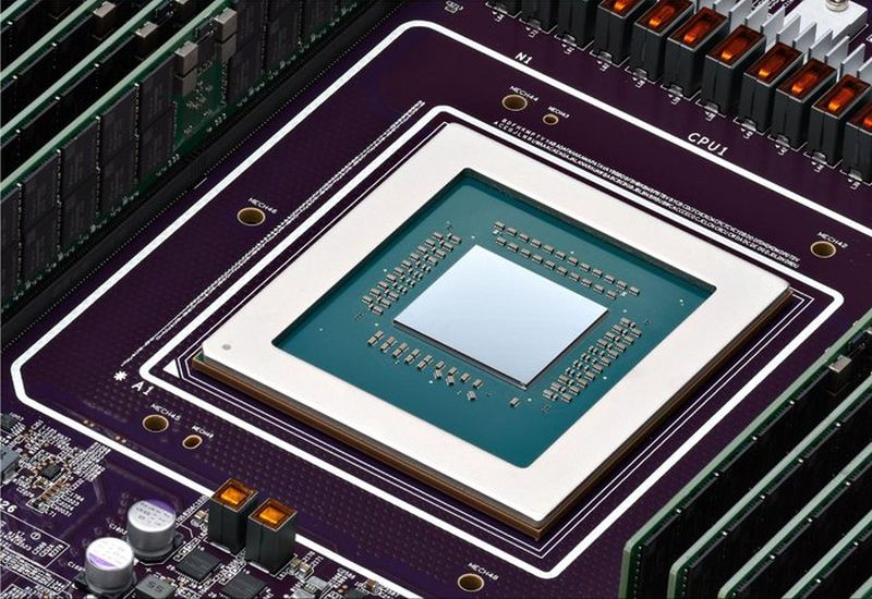
Image source: Google
In an increasingly competitive environment, such a high rate of development is necessary, how sure i am Amin Vahdat serves as Google’s Chief Technology Officer and Senior Vice President of Artificial Intelligence Infrastructure. These revelations were made during his speech at the Semicon Taiwan 2026 event. Last year, Google began updating TPU twice within a year. “I think the pace may even accelerate; the frequency of updates to our custom silicon solutions may increase,” – stated a company representative.
To achieve this, production lines are operating at full capacity and there is sufficient wafer testing capacity, he said. A company representative said that it is not only necessary to change the architecture of Google chips, but also to fundamentally change the way it works with the supply chain. As Wahdat acknowledged, there are bottlenecks in these chains, including the availability of memory chips, printed circuit boards, power supply components, liquid cooling systems, and even server racks as structural elements. As Vahdat points out, if this might be a problem at 10 a.m., then by lunchtime it’s a completely different problem. The industrial experience of the past few years tells him that he can never leave the problem area for a moment.
Google launched its first TPU tensor processor in 2015. This year, it released two chips at the same time: TPU 8t for training AI models and TPU 8i for inference. When designing the chip, special attention was paid to the integration of high-speed network data exchange channels so that cluster expansion can be as efficient as possible. Within its own infrastructure, Google can combine up to 1 million TPUs. Parent company Alphabet is preparing to allocate up to $205 billion this year to develop this infrastructure. TPU wafers will also be sold to third-party customers. Formal competition with Nvidia does not prevent Google from continuing to purchase the brand’s accelerators to meet its own needs.
Google also has strong manufacturing ties with Taiwanese partners. MediaTek is helping it develop the TPU chips, while TSMC is responsible for manufacturing. In terms of chip development, Google also cooperates with Broadcom and Marvell, which are themselves customers of TSMC. Taiwanese contractors assemble classic server systems for Google, but TPU solutions are only produced by Celestica and Flextronics in the United States. Google is preparing to allocate additional funds to expand its business in Taiwan by 60%. Intel and Samsung are also likely to participate in contract manufacturing, testing and packaging of Google chips. Taiwan is Google’s largest development base for artificial intelligence infrastructure solutions after the United States.
If you find an error, select it with your mouse and press CTRL+ENTER.