


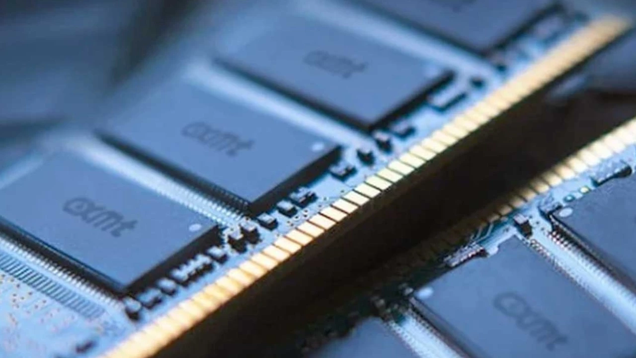

China’s Changxin Storage is trying to enter the HBM market, but the company’s production is still difficult. According to Korean media reports, the yield rate of available 8-layer HBM3 wafers is only 25-30%, seriously complicating mass production.
The main problem lies with TSVs, the vertical interconnects that pass through the silicon layer and allow interconnected dies to exchange data. There are approximately 3,000 in a CXMT chip. Manufacturers also have difficulty stacking and connecting DRAM crystals, which is why a large portion of the products fail final quality inspections. Industry insiders estimate that out of a batch of about 100 wafers, about 70-80 may be rejected.
HBM is significantly more complex than traditional DRAM due to the need to combine multiple layers of memory into a single stack. Current solutions use up to 16 layers, and future HBM4 will require more complex connection technologies. Changxin Memory previously consolidated its position in the global memory market by supplying traditional DRAM to Chinese companies, while Samsung, SK Hynix and Micron transferred a large amount of resources to HBM. Now, attempts to catch up with the leaders in this field have shown that the technical barriers to entry remain high.