

Taiwan’s TSMC’s technology leadership in foundry must be defended regularly as Intel and Samsung, with varying degrees of success, struggle to catch up. With Intel likely to begin trial production of components using 14A technology as early as the first quarter of 2027, TSMC will try to reach a similar level of readiness with its A14 during the same period.
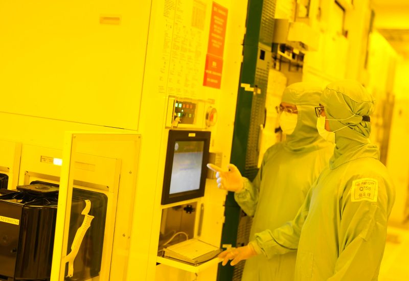
Image source: TSMC
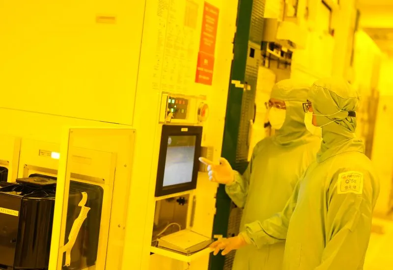
So far, it is believed that TSMC will master the mass production of wafers with A14 technology no earlier than 2028, but the experimental stage of producing components with new technologies is always mastered before mass production begins. as mentioned before business timesTSMC will start trial production of components using A14 technology at its Fab 20 plant in Hsinchu in the first quarter of next year. By the second quarter of 2027, the second Fab 25 factory in Taichung, currently under construction, will also be ready to start developing A14 technology. By the third quarter of 2027, Fab 25 will be able to begin trial production of wafers using A14 technology. TSMC still does not expect to begin mass production of chips using this technology until 2028.
In July, company representatives said the A14’s development progress was better than expected. During the production phase of the first prototype, the yield level of suitable products was close to 90%. SRAM memory cells, which are often used as prototypes when developing new technology processes, have shown similar levels of defects. Taiwan’s Fab 20 must switch from producing 2nm wafers to more modern wafers using A14 technology. Within the structure of this complex, the P3 building will focus on the production of specialized advanced products. Prototypes will be received in the first quarter of next year.
At the same time, the company will start mass production of wafers using A14 technology mainly in the new Fab 25 factory, which will be completed in April next year. Following the A14 technology process, chip production based on A12 and A13 technology will be mastered in 2029. The latter design rules will be compatible with A14, which will ease the transition for chip designers, and in A12, power will be provided on the reverse side of the silicon wafer (super power rail). Process flows A14, A13 and A12 belong to the same series and have a fairly long life cycle.
Meanwhile, Taiwanese sources Report Regarding TSMC’s plan to expand production using the technology processes it has mastered. By the end of this year, the production of 2nm products will reach 100,000 silicon wafers per month, and will increase to 140,000 silicon wafers per month by the end of 2027. In the fourth quarter of this year, the output of 3-nanometer products will reach 180,000 silicon wafers per month, and will exceed 200,000 silicon wafers per month in the next quarter. In other words, TSMC will use N2 and N3 technologies to expand production at the same time, and introduce A16 and A14 for trial production. Many of TSMC’s customers, including smartphone, server and PC chip makers, have already expressed strong interest in the latter.
As part of the A14 technology, TSMC will introduce new second-generation GAAFET transistor structures and NanoFlex Pro technology, which defines the architecture of standard semiconductor wafer cells. The latter can increase the density of transistors on a chip by reducing the gaps between cells. The previous generation NanoFlex architecture had been tested by TSMC as early as 2nm technology. Compared with N2, the transistor density of A14 should be increased by 20%, and the performance should be improved by 10% to 15% under the same power consumption, or the transistor density should be reduced by 25% to 30% under the same performance. TSMC’s two base factories in Taiwan will be able to process 70,000 silicon wafers per month using A14 technology, and will eventually open a third factory in southern Taiwan, as well as a US Fab 21 factory in Arizona.
If you find an error, select it with your mouse and press CTRL+ENTER.