


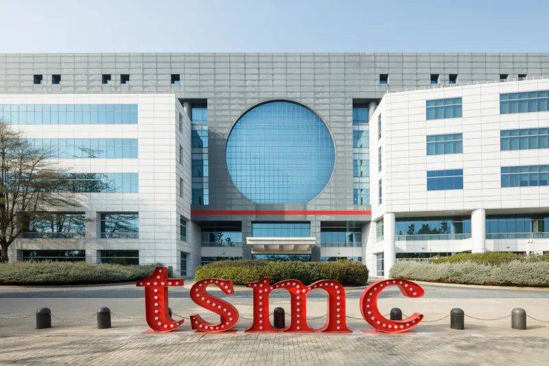
TSMC’s advanced enterprise in Taiwan has already gained momentum in the production of 2nm wafers on its assembly lines, but next quarter it is preparing to start mass production of semiconductor components using the more advanced A16 process technology, which can be considered 1.6nm in the conventional sense. The development and verification of the corresponding technology has been completed.
Image source: TSMC
According to Chosun Biz, the Taiwan version of “Liberty Times” reported on this this week. This technology process provides an important innovation – supplying power to the backside of the silicon wafer, called the Super Power Rail (SPR) in TSMC terminology. In this case, the signal circuits and the power circuits are separated, which makes it possible to reduce their mutual influence and increase the energy efficiency and speed of the chip. At the same time, the rules of chip design have not changed much, making it possible to speed up the development of new components.
Compared with the N2P version of the most advanced 2nm process technology currently produced by TSMC, A16 technology provides an 8-10% performance improvement while maintaining the same power consumption, or allows a 15-20% reduction in power consumption at the same speed. At the same time, the density of transistors increased by nearly 10%. The A16 process technology will be the first in TSMC’s arsenal to provide power from the backside of the chip. This technology will show its advantages in the production of large processors required in the field of artificial intelligence, as it will reduce power consumption while increasing the density of components on the wafer.
Gate adjacent (GAA) transistors were originally introduced as part of the N2 series of technologies and will continue to improve in the A16. In other words, this generation of TSMC technology standards will provide progress in two directions at the same time: in the fields of transistor architecture and power wiring. From a life cycle perspective, A16 will be a pass-through solution and TSMC is not making a big bet. People are looking forward to the more advanced A14, which is scheduled to achieve mass production of chips in 2028. In this case, power from the back of the crystal will also be provided.
TSMC maintains a clear advantage in the time it takes to master advanced lithography technology. Samsung Electronics will begin implementing SF1.4 no earlier than 2029, with a focus on increasing the yield of wafers available in the SF2 series of technologies. Intel has already provided 18A process technology to customers, but the more advanced 14A process will not begin mass production until 2028.
If you find an error, select it with your mouse and press CTRL+ENTER.