



Samsung Electronics is expanding its development of NAND flash memory for use in artificial intelligence systems. The company is working on three z-NAND options, each of which is focused on a specific type of workload: from local data processing on devices to work in high-performance data centers.
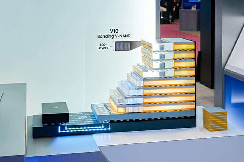
Image Source: Samsung Electronics
According to the South Korean publication ZDNetthe first type of memory is zNAND-O, which was announced by Samsung in August, designed to work with local AI. It is designed in such a way as to minimize delays in data transfer between neighboring components of computing systems. Unlike traditional methods, which transfer data to the external pins of the chip using wire connections, zNAND-O uses Through-Silicon Via (TSV) technology to allow four to eight NAND memory dies to be placed vertically. This shortens the data path, increasing speed and energy efficiency.
The second type, not yet officially announced, zNAND-T, focuses on throughput. zNAND-T memory is designed for use in powerful data centers where instant transfer of huge amounts of information is required. The architecture of this product is close to the concept of high-speed flash memory (HBF), providing a wide channel for data.
The third type, also not yet presented zNAND-I, is optimized for high speed random memory access (IOPS or number of input/output operations per second). This parameter is critical for AI inference tasks, where the system needs to constantly access small amounts of temporary data. An example is caching systems that require a high frequency of small requests.
Samsung Electronics’ decision to create three separate lines of NAND memory was dictated by requests from large technology companies for equipment customization. Competitors such as SK hynix are also developing their own AI memory families, separated by load type.
If you notice an error, select it with the mouse and press CTRL+ENTER.


